Resistivity research uncovers thin film star material

Imec’s Zsolt Tökei discusses the latest outcome of imec's research on binary and ternary alloys for advanced interconnect metallization schemes with Silicon Semiconductor’s Phil Alsop.
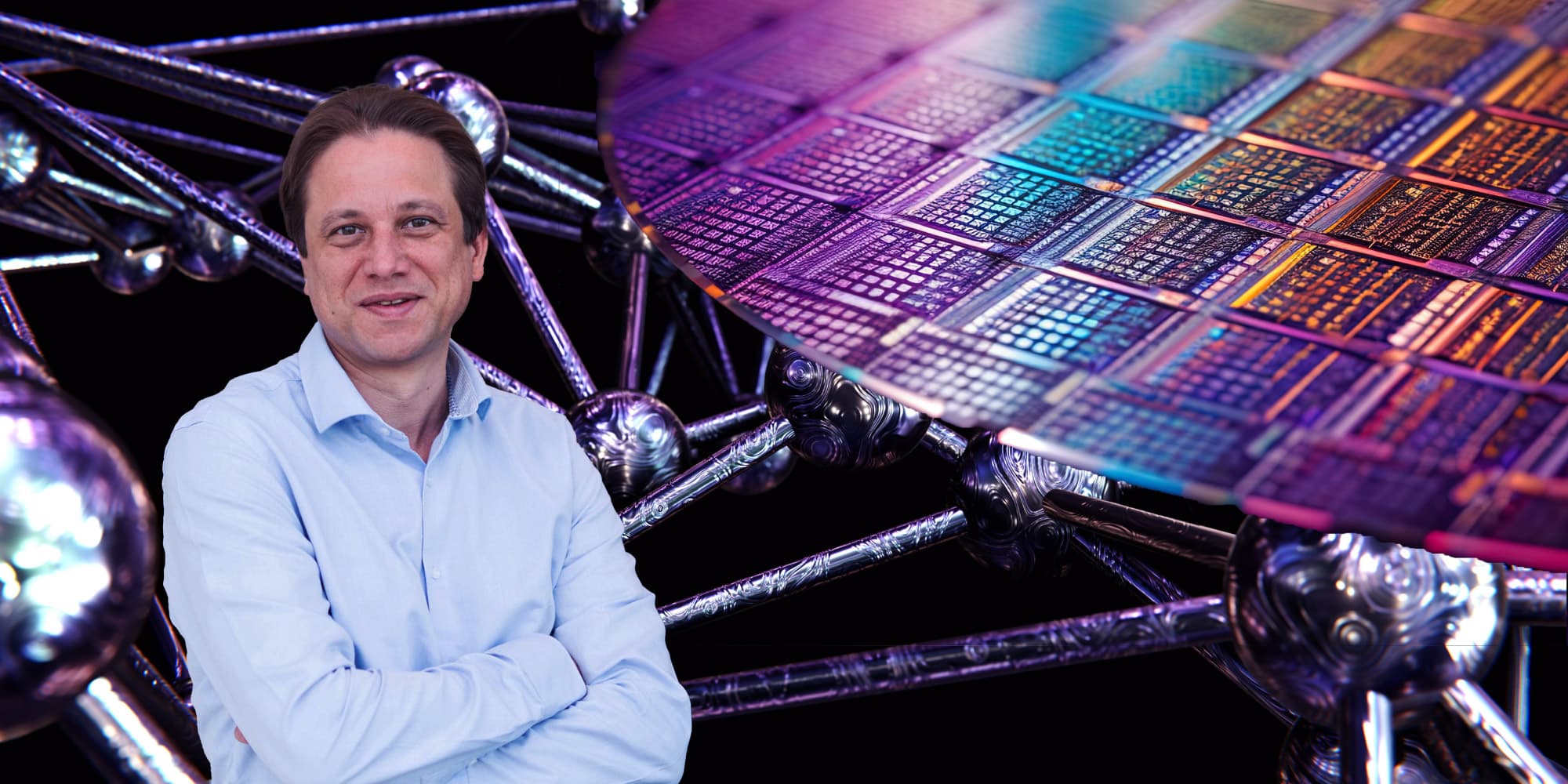
Portrait of a researcher in front of a colorful thin-film microchip graphic and metallic lattice structure

Zsolt Tőkei, fellow and program director of nano-interconnects at imec, explains the work behind the first experimental evidence that the resistivity of a thin conductor film on a 300mm silicon wafer can be lower than that of copper or ruthenium. Zsolt explains the research methodology of the project, commenced in 2016, and shares his excitement as to how the research will identify and categorize various binary and ternary alloys that can outperform copper and ruthenium when it comes to interconnect lines.

The old "videoblock" block was not automatically migrated. The old video embed is not a supported YouTube, Vimeo, or Dailymotion URL. Editors should manually revisit this page.

Source content: https://www.imec-int.com/en/articles/resistivity-research-uncovers-thin-film-star-material

This video was originally published in Silicon Semiconductor.

Authors

Portrait of Zsolt Tokei standing with arms crossed in front of large office windows

Zsolt Tokei

Imec fellow and incoming program director of 3D system integration
Author

Zsolt Tokei is Distinguished Member of Technical Staff Interconnects at imec. He joined imec in 1999 and since then held various technical positions in the organization. First as a process engineer and researcher in the field of copper low-k interconnects, then he headed the metal section. Later he became principal scientist, Program Director Nano-Interconnects and, in 2016, was appointed Distinguished Member of Technical Staff Interconnect. He earned a M.S. (1994) in physics from the University Kossuth in Debrecen, Hungary. In the framework of a co-directed thesis between the Hungarian University Kossuth and the French University Aix Marseille-III, he obtained his PhD (1997) in physics and materials science. From 1998 he worked at the Max-Planck Institute of Düsseldorf, Germany, as a post-doctorate researcher. From the date of joining imec he continued working on a range of interconnect issues including scaling, metallization, electrical characterization, module integration, reliability and system aspects.
Read more about this author

Discover more

Stylized 3D rendering of an imec research building at night with a glowing logo

Europe’s pilot line to enable future compute systems

21/10/2024
Vision
CMOS: advanced & beyond
NanoIC pilot line
Interconnects
Read more
Glowing blue circuit traces radiate from a central microchip on a dark motherboard

Cross-technology co-optimization (XTCO)

Page
CMOS: advanced & beyond
Read more
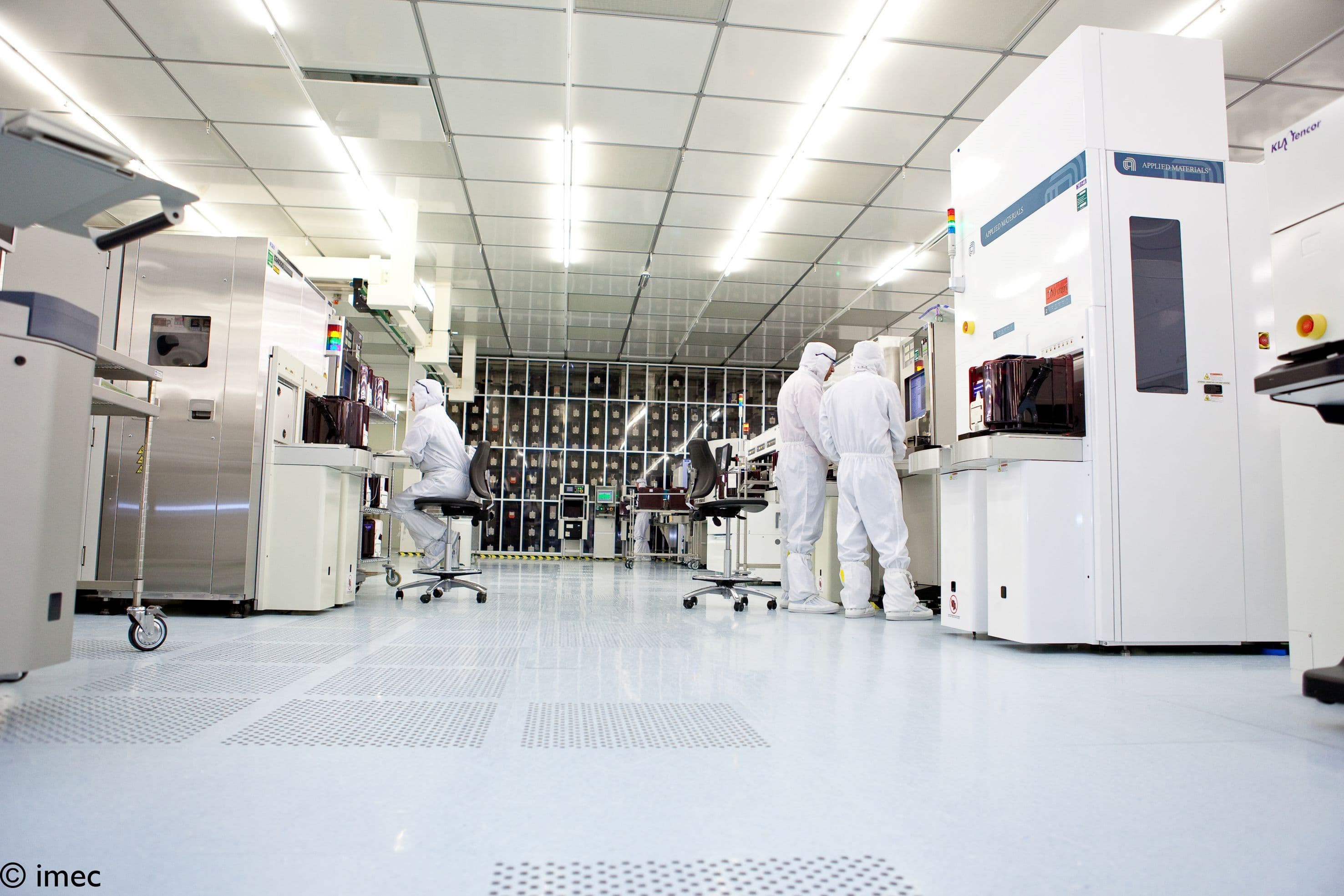
Cleanroom with researchers in white suits working beside semiconductor equipment

Semi-damascene metallization: inflection point in back-end-of-line processing?

31/10/2024
Page-turner
Interconnects
CMOS: advanced & beyond
Read more
Blue abstract illustration of curved semiconductor wafer sections and chip-like patterns

White paper: monolithic microsystems

Page
Sensing and actuation
CMOS: advanced & beyond
Read more
Illustration of Earth connected by glowing data streams to microchips, wafers, and server racks

How hyperscalers are rethinking AI infrastructure

06/08/2026
Technology review
Interconnects
Data- and telecom
Read more
Gloved hands holding a printed chip layout with multiple die blocks

When does it make sense to move from a monolithic ASIC to a chiplet-based design?

23/06/2026
Longread
CMOS: advanced & beyond
Artificial intelligence
Read more
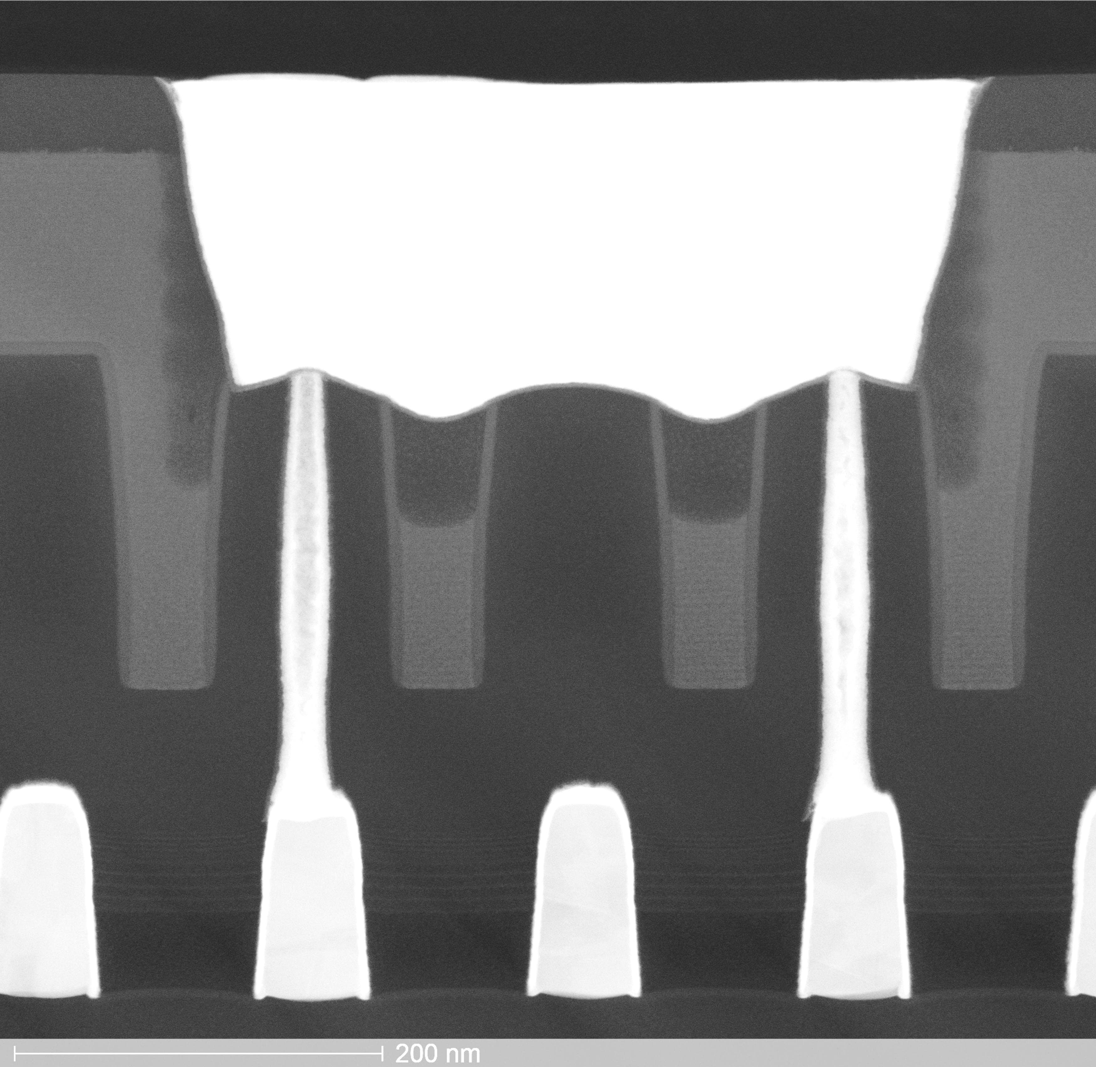
Cross-sectional micrograph of a chip structure with vertical interconnects and a 200 nm scale bar

Sony and imec unveil high-density backside connectivity module enabling next-generation 3D chip integration

16/06/2026
press release
CMOS: advanced & beyond
Read more
Groene lichtpuntjes verspreid over horizontale lagen, als een abstract beeld van vloeistofgeheugen

ASML, TSMC and imec bring industry-ready 2D-material transistors closer with breakthrough 300mm integration

15/06/2026
press release
CMOS: advanced & beyond
Read more
Imec building exterior under a blue sky with sunlight reflecting off the facade

Imec launches university consortium around next generation of chips

12/03/2026
press release
CMOS: advanced & beyond
Academic Excellence
Read more

imec in your region

Looking for information about imec's activities in different parts of the world?

United Kingdom
United States
Qatar