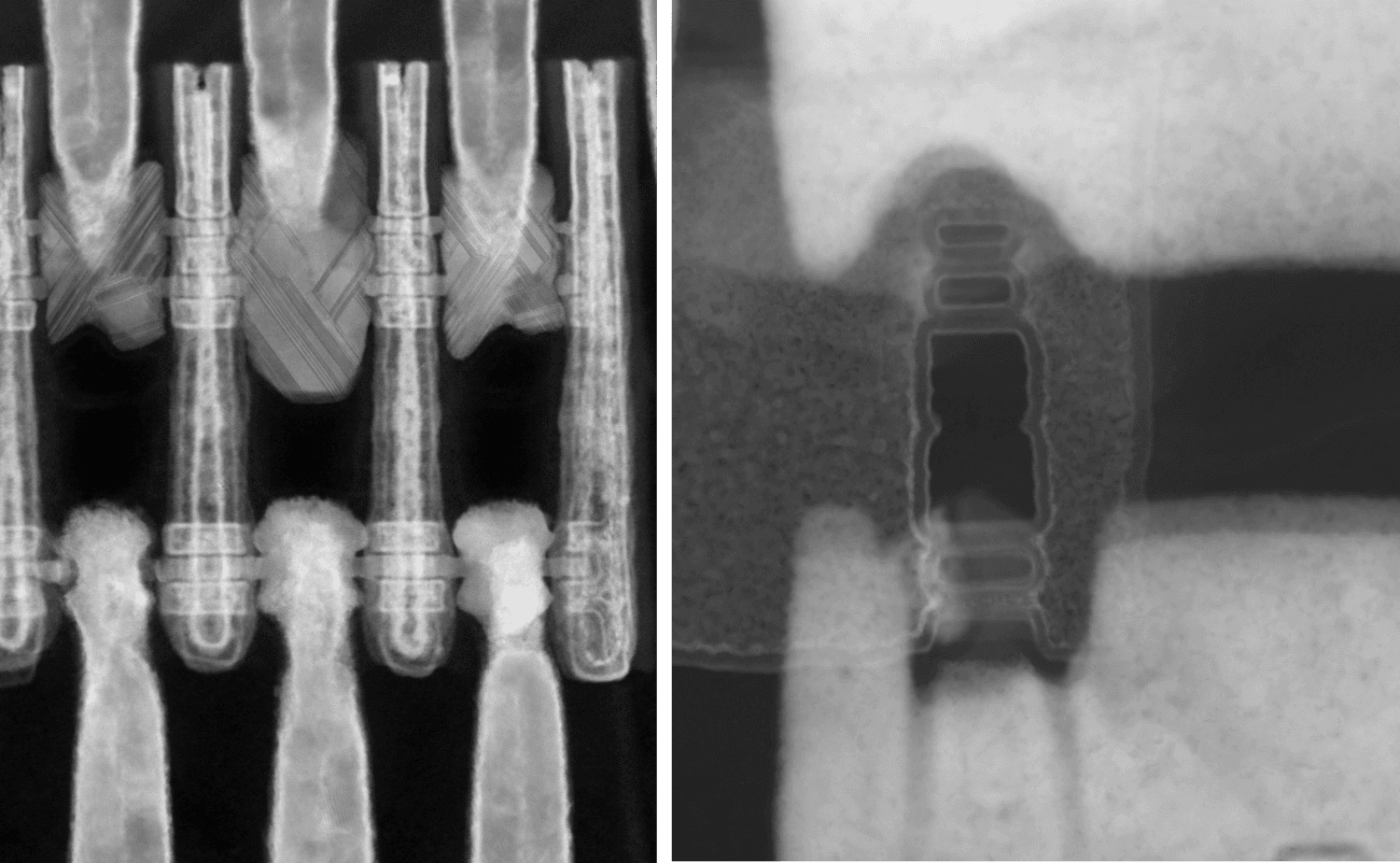
Imec brings magnetic domain wall devices closer to industrial reality
Unique design enables full electrical control, paving the way to both logic and memory nano-device operation
In short
Magnetic domain wall devices have attracted great attention as a promising beyond-CMOS device concept for functional scaling. The spintronics-based technology could provide a platform where both logic and memory might connect, holding promise for logic-in memory computing as well.
In this article, Eline Raymenants, Van Dai Nguyen and Inge Asselberghs present a unique device concept that provides full electrical control – thereby overcoming the practical hurdles for making CMOS-compatible nanoscale domain wall devices.
Their work is reviewed in a 2021 invited IEDM paper, which provides an additional outlook towards realizing industry-relevant complex domain wall logic circuits.
The promise of magnetic domain wall devices for logic and memory applications
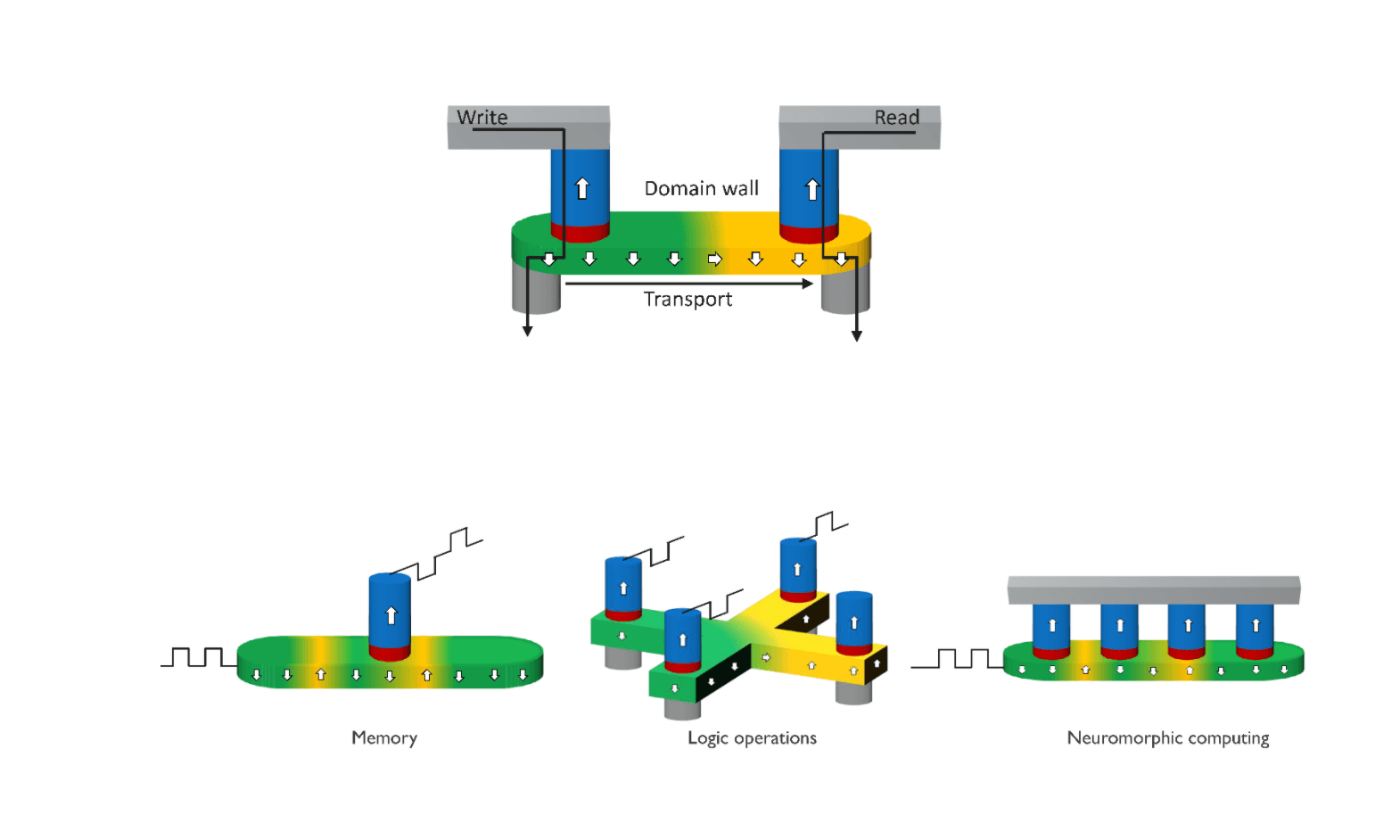
While the semiconductor industry continues to push Moore’s law into the next decade, research institutes and academia worldwide explore ways beyond dimensional scaling to pack more functionality per area. A promising approach for functional scaling is a domain wall device: a device that encodes information in magnetic domains. Neighbouring magnetic domains with different magnetization (denoted as ‘1’ or ‘0’) are separated by magnetic domain walls. The ability to read and write these domains and to transport the domain walls from input to output provides an interesting basis for building both logic and memory devices.
A prerequisite for logic applications is the ability to transfer information between input and output and between different logic gates at a very high speed. This requires fast motion of the domain walls within a track of magnetic material. Under this condition, they can be used as building blocks for majority gate devices or even more complex logic circuits. Majority gates are ‘democratic’ devices that return ‘true’ (or ‘1’) if more than 50% of their inputs are true. In their most simple implementation, they use three inputs and one output.
In the context of memory, domain wall devices have been earlier proposed as enablers for racetrack memory – a non-volatile memory concept where domain walls are routed through a magnetic track towards a selected number of write and read elements. These memories can potentially reach extremely high density, a metric that is now solely determined by the material used for the magnetic track.
Having thus a platform where both logic and memory can connect (along the same magnetic track) offers a way to go beyond the traditional Von Neumann architecture, where data storage and computation are physically separated. This implies that the technology holds promises for neuromorphic in-memory computing as well.
The challenge: all-electrical read and write concepts
The idea of using magnetic domain wall devices for logic and memory applications goes back several decades. Experts in spintronics have explored different device concepts, both theoretically and in the lab. However, their work mainly focused on exploring mechanisms in different materials to enable efficient and fast domain wall motion. Meanwhile, there was less innovation in renewing methods for electrically reading and writing the domain walls at nanoscale. They mainly relied on the use of external magnetic fields for writing, and magnetic imaging techniques for the reading.
When targeting scalable, CMOS-compatible devices for logic and memory, full electrical control of nanoscale domain devices is however essential. An attractive approach is the use of magnetic tunnel junctions (MTJs) for electrical reading and writing. MTJs have intensely been researched and optimized in the context of magnetic random-access memory (MRAM) technology development. They consist of a thin dielectric layer (MgO) sandwiched between a magnetic fixed layer and a magnetic free layer. The spin-transfer torque (STT) variant of MRAM uses a current to switch the magnetization of the free layer (usually ferromagnetic CoFeB). Reading is performed by measuring the tunnel magnetoresistance of the MTJ by passing a current through the junction.
Although excellent for reading and writing, traditional STT-MRAM material stacks pose severe limitations for practical domain wall device operation. In ferromagnetic CoFeB, the domain wall speed is too low to be applicable for logic applications. In addition, challenges remain with respect to the etch patterning steps in the MTJ ‘pillar’ manufacturing process. The CoFeB layer is very susceptible to etch damage, which would additionally hamper transport of the magnetic domain walls within the track.
Imec’s approach: an MTJ stack with hybrid free layer
Imec has overcome the challenges for the practical realization of domain wall devices, offering a complete set of components to read, write and transport information electrically and to build industry-relevant devices. Key innovation is the design of a hybrid free layer: a second free layer specifically for domain wall transport is incorporated into a conventional MTJ stack. The new design takes advantage of both MTJ technology development (for efficient read and write operations) and transport material optimization (for fast domain wall motion).
The first free layer (CoFeB) is used for efficiently writing the domains through STT, with which the domain walls are also injected into the second free ‘transport’ layer. This layer can be a ferromagnet or an antiferromagnet (such as Pt/Co/Ru/Co). An extra spacer in between the free layers enables an efficient ferromagnetic coupling between both layers. The domain walls then travel along the shared track at high speed, driven by spin-orbit torque (SOT). Detection at the output (reading) is enabled by reliable tunnel magnetoresistance.
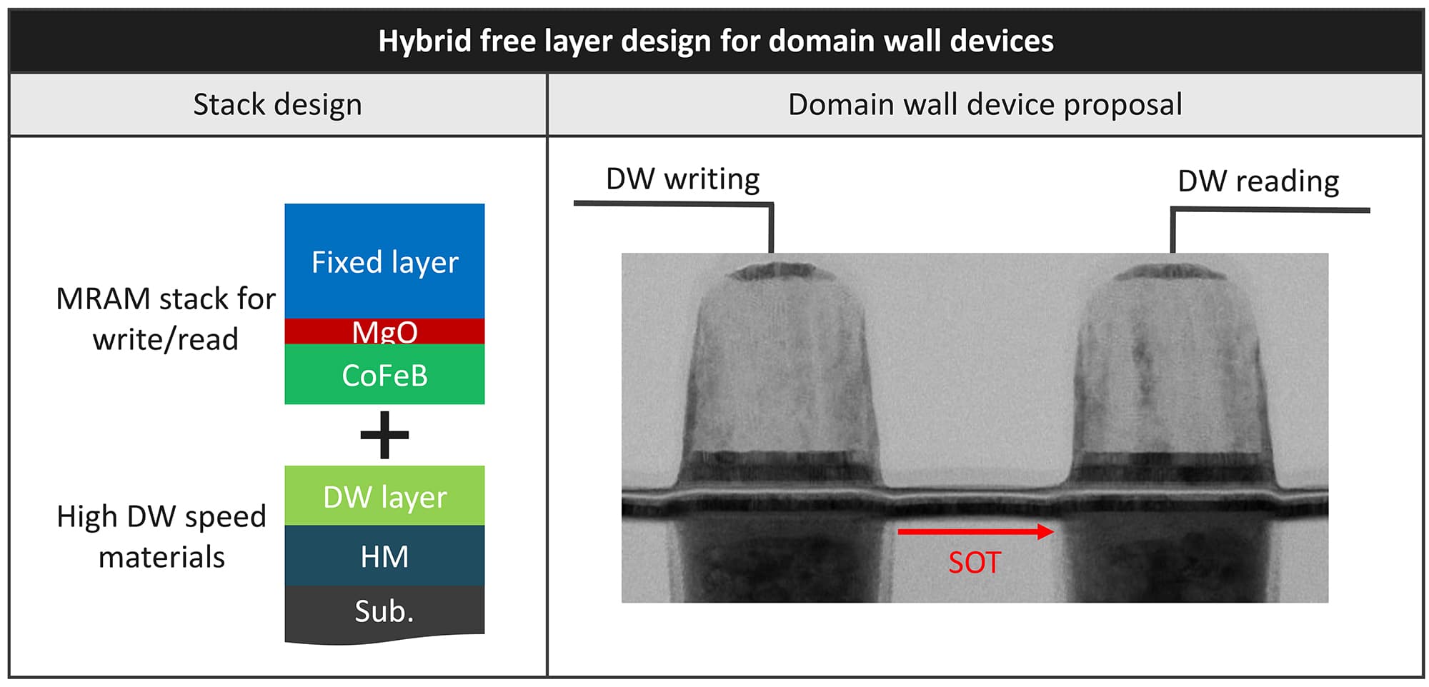
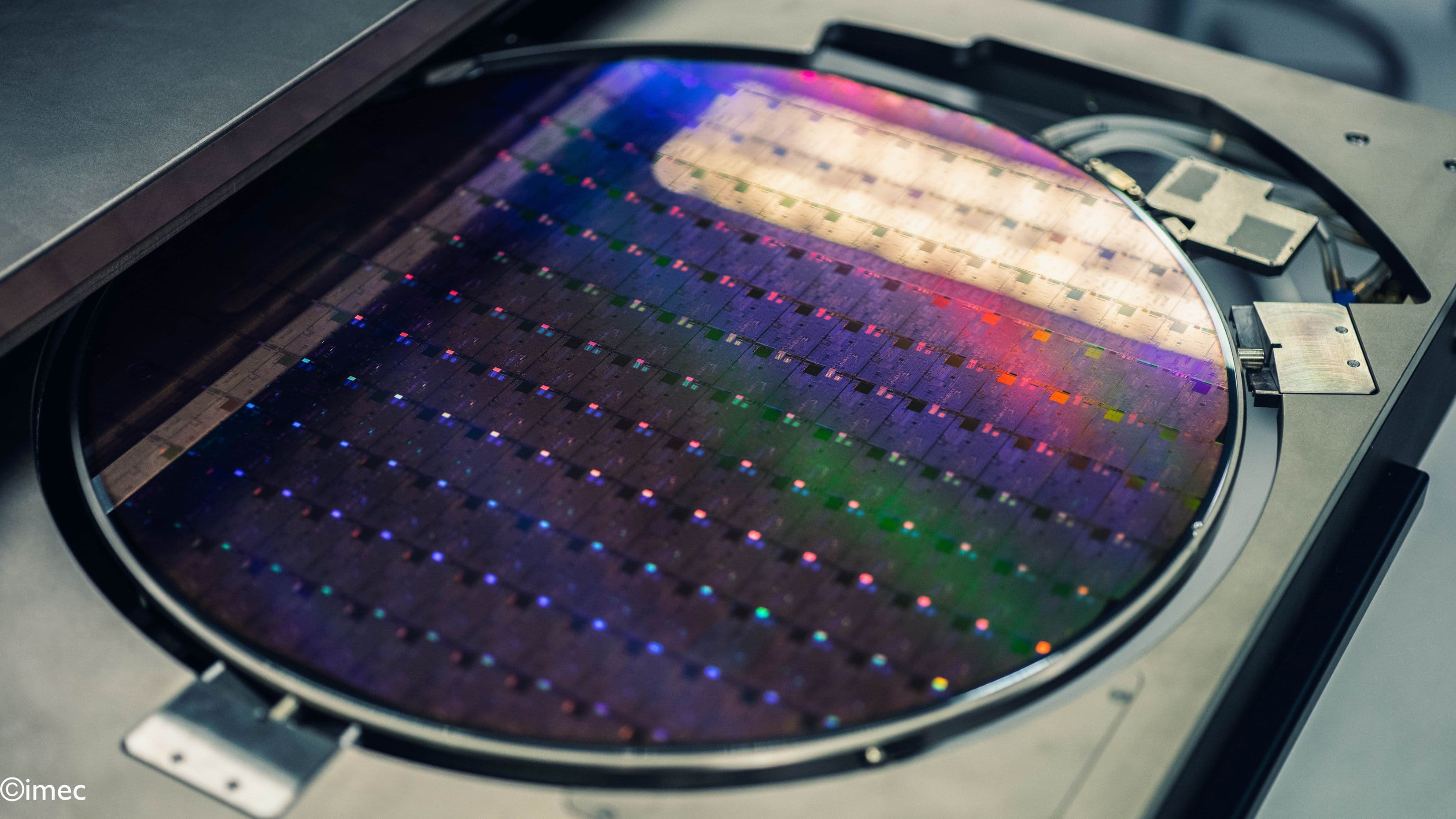
This new all-electrical concept also allows to overcome the key integration challenge related to the MTJ etch patterning step. Even if the first layer is damaged by the patterning step, the domain walls can still move inside the bottom transport layer which is more shielded from the etching step. In addition, the devices are built in imec’s 300 mm wafer facility, using standard processes of MRAM technology – largely facilitating industrial adoption of the technology.
At 2020 IEDM, the imec team presented the first proof of concept of using these magnetic domain wall devices for logic applications. Several MTJs, acting as logic inputs, were configured to feed simple AND and OR logic gates.
These recent developments are reviewed in the 2021 IEDM invited paper ‘Magnetic domain walls: from physics to devices’ by E. Raymenants et al. Key results have also been described in the Nature Electronics paper ‘Nanoscale domain wall devices with magnetic tunnel junction read and write’ by E. Raymenants et al.
Outlook: towards fully functional, real-world logic, memory and logic in-memory circuits
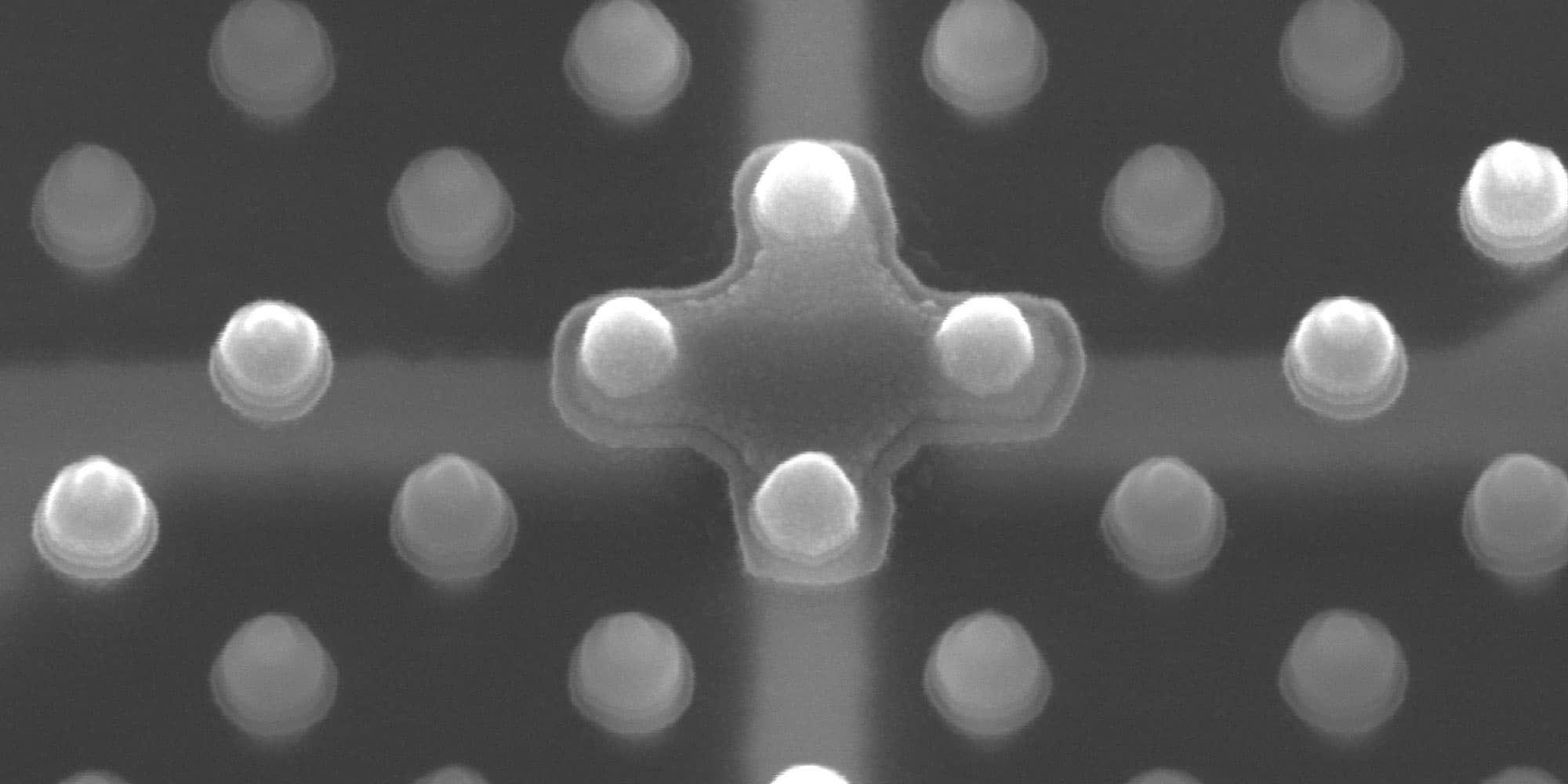
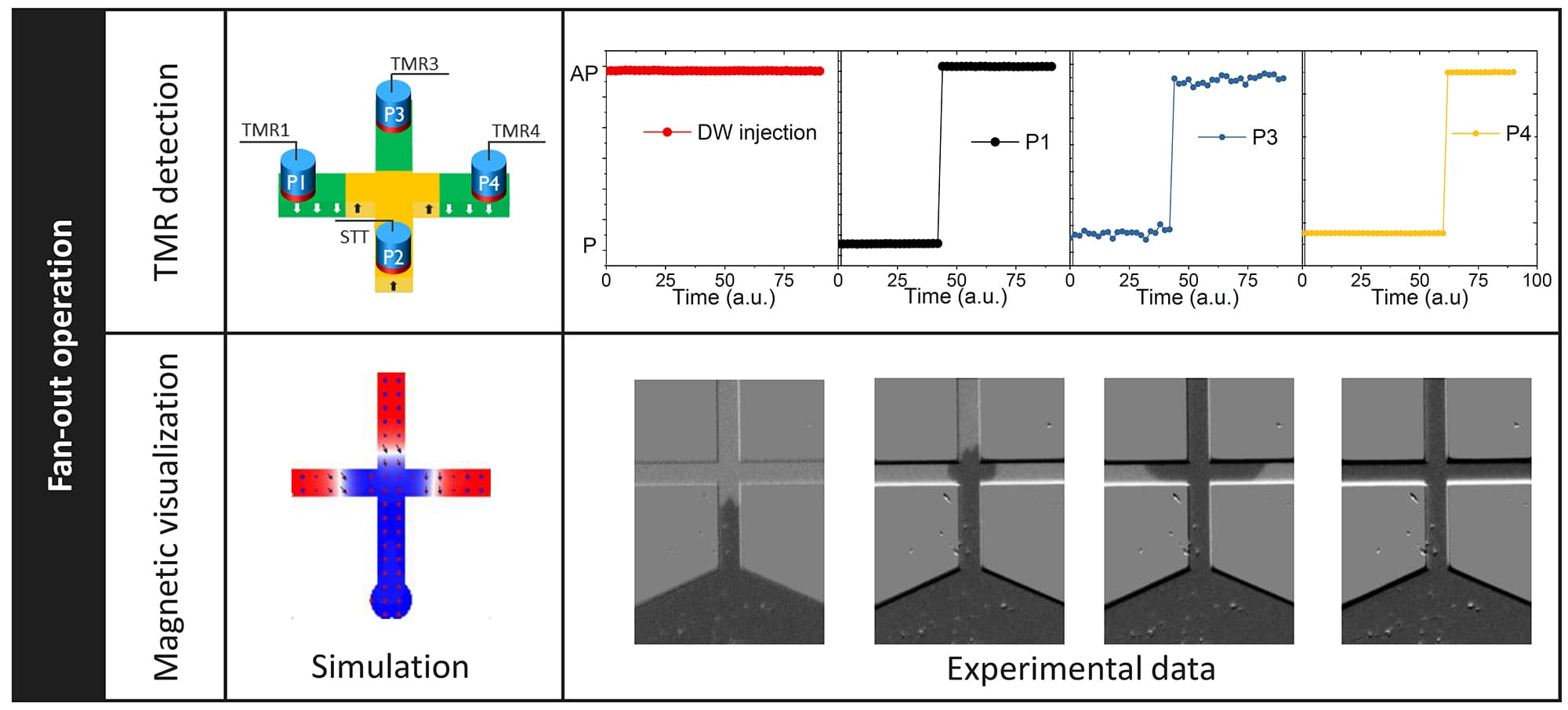
There is still a long way to go before magnetic domain wall devices can be brought into commercial products. The 2021 IEDM paper describes the team’s first steps towards building more complex beyond-CMOS logic circuits. In this study, the basic building blocks presented above are implemented in more complex logic geometries to learn more about the domain wall motion within these structures. An example of such a geometry is an implementation of a spin torque majority gate (STMG), consisting of three input MTJs and one output MTJ. The four MTJs share a cross-shaped domain wall track. The team could not only demonstrate domain wall motion within the track (in agreement with observations by magnetic imaging), they could also prove that this design enables fan-out operation. Fan-out operation means that the output signal of one or more logic gates can be used as the input signal for adjacent gates – a key requirement for logic circuit operation.
Additional research is planned to prepare for fully functional high-density racetrack memory. In the future, new architectures and algorithms for domain-wall-based logic-in memory devices will need to be developed as well.
Conclusion
At 2021 IEDM, imec reviews its work on magnetic domain wall devices intended for both logic and memory functional scaling, and for neuromorphic computing. A novel free layer design within the MTJs is demonstrated to overcome the practical limitations of state-of-the-art magnetic domain wall devices. Initial research into implementing the devices in more complex logic circuits looks promising, paving the way towards energy-efficient spintronics devices for beyond-CMOS logic applications.
Acknowledgments
This work was performed as part of the imec IIAP core CMOS program and Beyond CMOS program of Intel Corporation. A part of this work was carried out in collaboration with Univ. Grenoble Alpes/Néel Institute, Grenoble, France.
Want to know more?
- Interested in receiving the 2021 IEDM paper ‘Magnetic domain walls: from physics to devices’ by E. Raymenants et al? Fill in our contact form.
- Follow imec's presence at the 2021 IEEE International Electron Devices Meeting
- Further reading on this topic:
- ‘Imec and Intel researchers develop spintronic logic device’, IEEE Spectrum, 2021;
- ‘The electrical control of domain wall devices based on perpendicular magnetic tunnel junctions’, TechExplore; 2021;
- ‘Nanoscale domain wall devices with magnetic tunnel junction read and write’ by E. Raymenants et al., Nature Electronics, 2021;
- ‘A domain wall device with electrical control’, News & Views, Nature Electronics, 2021.
Authors

Eline Raymenants
Eline Raymenants is PhD student at imec and KU Leuven, Belgium. She received the M.Sc. degree in nanosciences, -technology and -engineering from KU Leuven, Belgium, in 2016. She is currently finalizing her PhD thesis where she studied the physics of domain wall dynamics in nanoscale devices and its applications for Beyond CMOS devices.

Van Dai Nguyen
Van Dai Nguyen is a Senior Researcher specializing in magnetic devices at imec. He earned his Ph.D. in Nanophysics from the University of Grenoble Alpes, France, in 2012. Following a postdoctoral fellowship focused on magnetic domain wall and MRAM devices at the Neel Institute and Spintec in Grenoble, he joined imec in Leuven in 2018. Currently, he leads research on the large-scale integration of Spin Orbit Torque MRAM on 300 mm wafers for memory applications.

Inge Asselberghs
Inge Asselberghs is program manager for exploratory logic at imec. She received the M.Sc. and Ph.D. degrees in chemistry from the University of Leuven, Leuven, Belgium, in 1998 and 2003, respectively. After a Post-Doctoral Fellowship in nonlinear optics, she moved to imec, Leuven, as a Researcher, where she was involved in exploratory 2-D-material-based device fabrication and characterization.
Discover more