A close look at iSiPP200, IC-Link’s integrated photonics platform
When we recently announced the expansion of IC-Link’s services portfolio, one element immediately caught our customers’ attention: the addition of a mature integrated photonics manufacturing platform.
It’s easy to see why. The ability to add an advanced photonic chip to a product is appealing to innovators across a wide range of industries — from datacom and AI to medtech, fintech, and automotive. Gaining access to photonic integrated circuit (PIC) manufacturing through a trusted supplier such as IC-Link, leveraging the best-in-class tech of imec, presents an exceptional opportunity.
So, let’s take a closer look at iSiPP200, IC-Link’s 200mm silicon photonics platform. What does it offer? And how can you access it?
20 years of silicon photonics expertise
First, a bit of history.
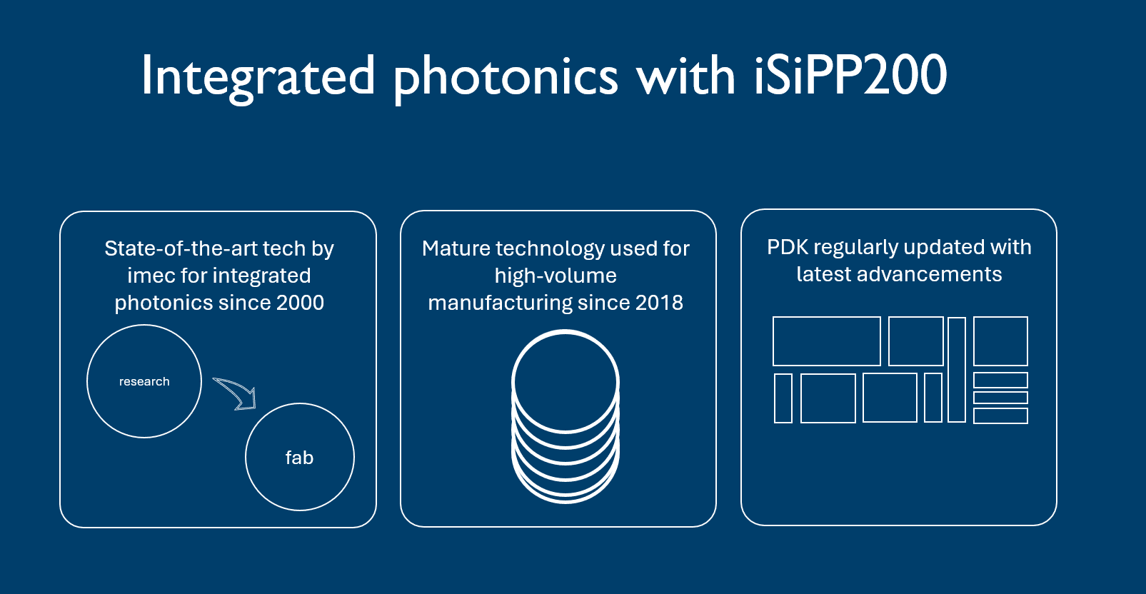
Imec’s work in silicon photonics dates back to 2000, when a dedicated research program was established. This program continues today, exploring – in close collaboration with industrial partners – how advanced optical I/O can enable system-level performance scaling.
Since 2018, the mature technology blocks developed through this program have been available for high-volume manufacturing. Today, an extensive and continuously updated PDK enables customers to design advanced PICs that smoothly transition into manufacturing without volume limitations.
What’s included in the PDK? The 200G device library
The latest PDK for the iSiPP200 platform provides a broad portfolio of devices supporting 200 Gbps per lane, enabling 800G and 1.6T pluggable optics, enabling hyperscale data centers and AI clusters.
Passive devices
- High-density silicon waveguides with average propagation loss of 0.5-2 dB/cm
- PECVD silicon nitride (SiN) waveguides; LPCVD SiN waveguides are available for prototyping and low-volume manufacturing
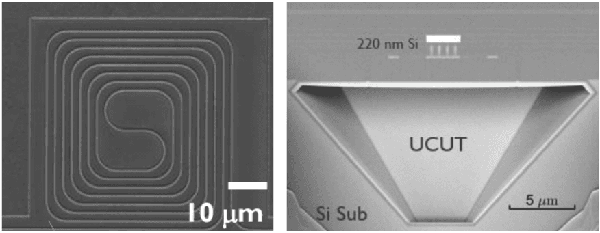
- Undercut structures for tripled heater efficiency and improved mode confinement
- Single-mode-fiber (SMF) grating couplers with less than 2 dB coupling loss
Active devices supporting 200G per lane
- Silicon ring modulators
- GeSi electro-absorption modulators for short-reach interconnects
- Silicon Mach-Zehnder modulators
- Ge photodetectors for monitoring transmitters or for high-speed performance in transceivers
3D/back-end features
- Cu-Ni-Sn under-bump metallization (UBM)
- Up to 4 metal layers
All devices undergo rigorous reliability testing, including high-temperature operating life (HTOL) and damp-heat testing.
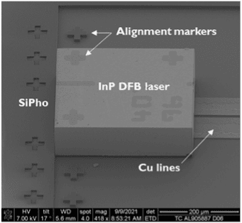
For additional functionalities, LNO modulators, III-V lasers and SOAs can be integrated through micro-transfer printing. InP lasers can be added through wafer-scale flip-chip bonding as well, depending on heat-sinking requirements.
On our way to 400G
As noted, iSiPP200 originated from imec’s pioneering research, and its close link to the world’s leading semiconductor R&D hub continues to be a defining strength of the platform.
There’s a clear trend towards higher data rates and shorter interconnect distances. That’s why we’re expanding our portfolio with devices supporting 400 Gbps/lane, enabling 3.2T pluggable optics:
- Lithium niobate (LNO) modulators
- High-speed Ge-on-Si photodetectors
- LPCVD SiN waveguides, fully integrated with the LNO modulators and Ge photodetectors
- A fully 3D-compatible platform
Additional innovations in development include compact, low-power passives for wavelength division multiplexing (WDM), low-power switches, pluggable connectors, TSVs, and optical interposers — all paving the way for co-packaged optics and advanced optical interconnects.
Ready to manufacture your PIC with iSiPP200 wafer services?
Our PDK, with its design rules and device library is your starting point for manufacturing PICs on the iSiPP200 platform. It enables you to start designing immediately, while IC-Link works on the process control monitoring (PCM) test structures that can be measured before wafer delivery to ensure quality and process integrity.
Once your design is finalized, IC-Link manages all prototyping and manufacturing steps.
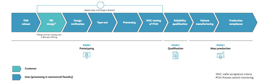
And to make PIC manufacturing as straightforward as ASIC manufacturing, we’re in the process of expanding our portfolio with design and packaging/assembly services. We’re now accepting selected projects to get started.
Want to know more?
Discover more