IC-Link by imec: unlocking market-ready semiconductor technology
Imec is known as the semiconductor R&D hub where companies come to develop technologies that will hit the market in 3, 5 or even 10 years’ time. In contrast, imec’s IC-Link division looks at what is already available: the incredible possibilities in cutting-edge chips hitting the market —today.
For decades, IC-Link, imec’s services division, has been a trusted partner for bringing ASICs (application-specific integrated circuits) from idea to commercial-grade silicon. Much of the work up to now has centered around ASICs in CMOS technologies.
Now, IC-Link’s offering is significantly expanding. Companies looking to incorporate advanced chips into their products will find it easier than ever to get access to best-in-class technologies, matured from imec R&D, and ready for manufacturing.
Evolving semiconductor landscape requires fresh-to-market tech
Up to now, IC-Link has been known as the enabler for companies looking to develop and manufacture ASICs in CMOS technology—even at the most advanced commercially available nodes. It offers full-turnkey services that cover the complete ASIC process, from technology selection, chip design and IP integration to silicon manufacturing, packaging, testing, qualification and supply chain management.
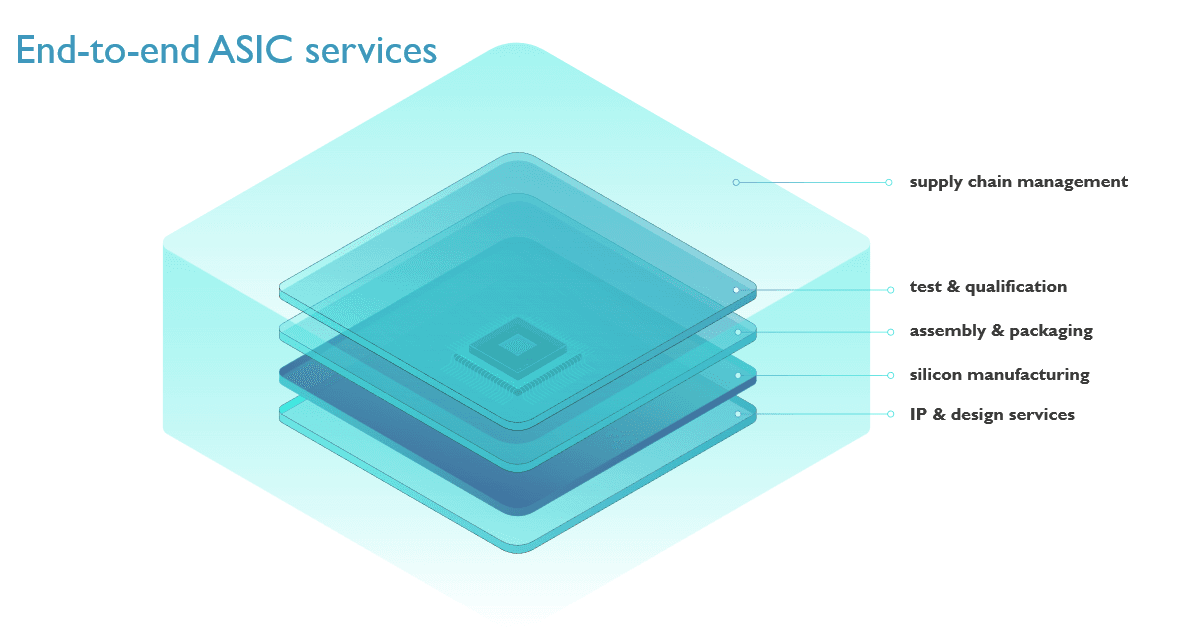
However, the semiconductor landscape is evolving. Deep-tech innovation is accelerating, and companies today face new challenges. To meet the changing landscape, we mature imec’s best-in-class technology into features fresh to the market that cannot be found elsewhere.
Continuously expanding IC-Link offering
To help our customers meet these challenges and ensure that breakthrough technologies mature beyond research and into commercial viability, IC-Link will greatly enlarge its offering with:
- An increased ASIC services portfolio – Adding extra in-house services, including designers with experience down to TSMC N2 and new testing capabilities along with internal advanced packaging design experience.
- Hardened IP – Investing in research-driven innovations and making them commercially deployable, including future automotive IP to be developed at the Advanced Chip Design Accelerator in Baden-Württemberg.
- Next-generation technology platforms – Moving beyond CMOS by introducing commercially validated imec technology platforms such as:
- Imec’s advanced integrated photonics platform, already a workhorse for tech innovators in data, telecom, and AI.
- Ultra-low-loss silicon nitride, set to join IC-Link’s portfolio in Q4 2025, enabling best-in-class PICs for quantum, sensors and biophotonics applications.
- 3D integration services –Based on imec's long-standing R&D program, these will be added in the future.
- Specialty technologies – Offering manufacturing capabilities, such as those that require post-CMOS processing, non-standard process steps and fine-resolution-pattern wafers with a direct path to volume production of technology demonstrators developed at imec, e.g. custom sensors and detectors.
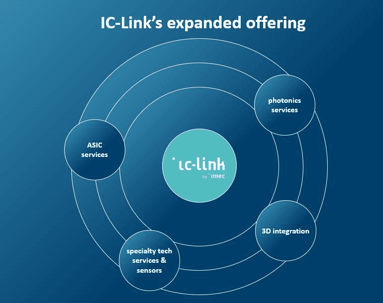
Plus, the offering will evolve in the future, as best-in-class technology from R&D is ready to be matured to go to market. This way, IC-Link is poised to become a key enabler of customized solutions for innovative chip manufacturing.
Want to discuss your custom chip product? At IC-Link, you’ll find features that are not available elsewhere. Click the button below to get in touch and discover what this could mean for you.
Discover more