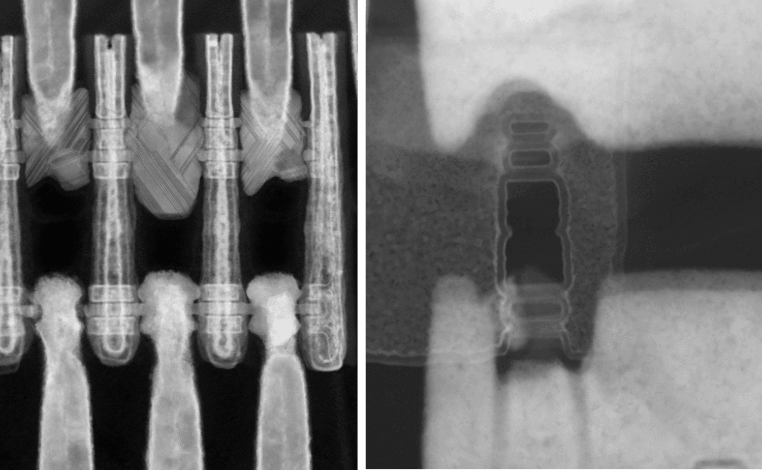
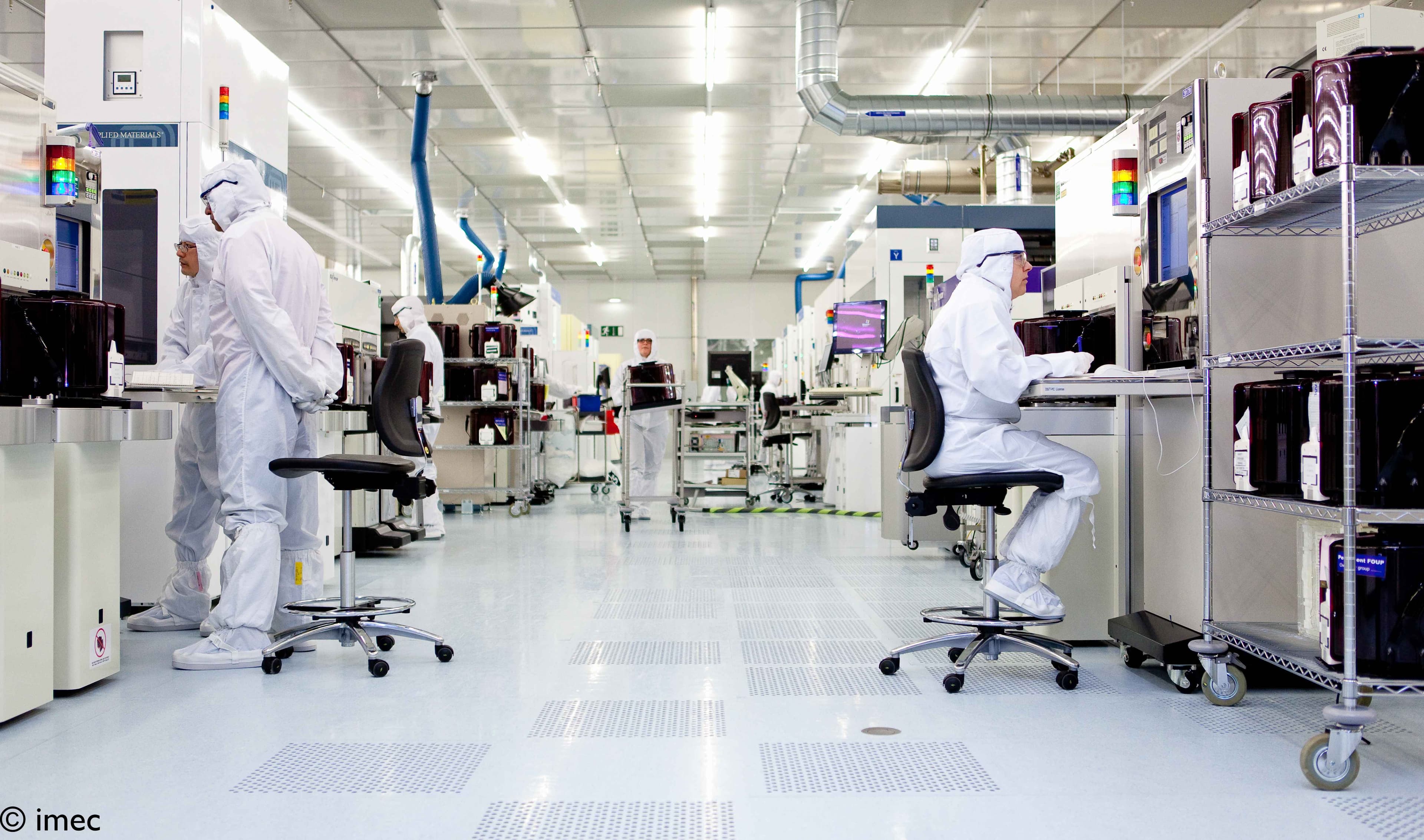
2D transistors look to extend the logic roadmap

Compound Semiconductor highlights imec’s work on 2D-material-based transistors
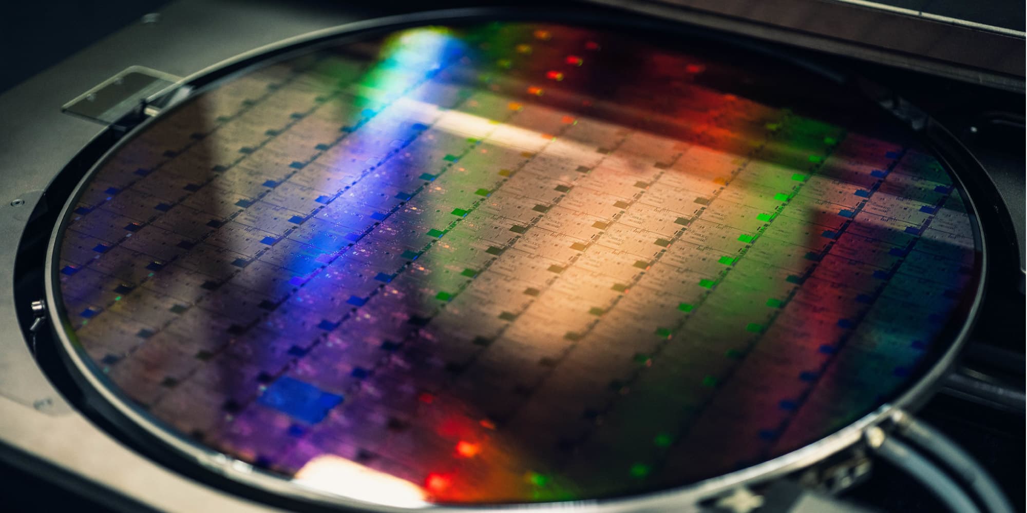
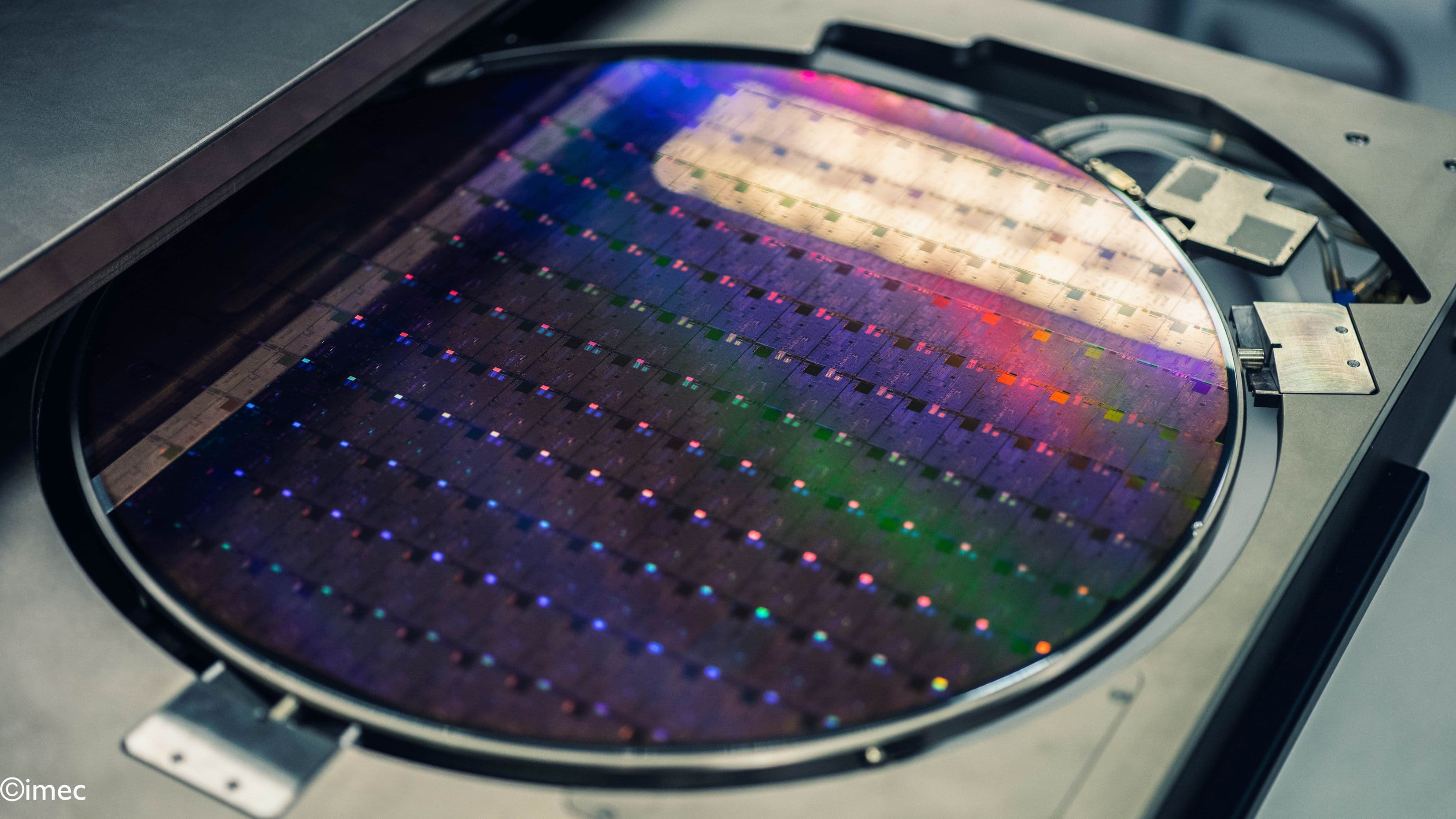
Silicon wafer with iridescent reflections under inspection, showing a patterned semiconductor surface

In short

2D semiconductors like tungsten disulfide (WS2) could extend the logic transistor scaling roadmap. 

Imec lays the groundwork for integrating these 2D materials in a 300mm CMOS fab, and works towards improved device performance.
 

Read the full article in Compound Semiconductor, Volume 27, Issue 4, pg 40-43.  

Authors

Portrait of Inge Asselberghs in a white jacket against a blurred outdoor background

Inge Asselberghs

Program Manager for exploratory logic at imec
Author

Inge Asselberghs is program manager for exploratory logic at imec. She received the M.Sc. and Ph.D. degrees in chemistry from the University of Leuven, Leuven, Belgium, in 1998 and 2003, respectively. After a Post-Doctoral Fellowship in nonlinear optics, she moved to imec, Leuven, as a Researcher, where she was involved in exploratory 2-D-material-based device fabrication and characterization. 

Read more about this author
Iuliana Radu smiling in a portrait with a blurred lab background

Iuliana Radu

Program Director responsible for exploratory logic activities at imec
Author

Iuliana Radu is program director at imec, where she is leading the beyond CMOS and quantum computing activities. Prior to joining the logic program at imec in 2013, she was a Marie Curie and FWO fellow at KU Leuven and imec. Her work at imec and KU Leuven includes devices using the metal-to-insulator transition, ionic and electronic transport in functional oxides and devices with graphene and other 2D materials. Iuliana has received a PhD in physics from MIT in 2009 where she worked on the fractional quantum Hall effect and searched for non-abelian quasiparticles.

Read more about this author

Discover more

Microscope close-up of stacked transistor structures in a CFET device cross-section

Performance boosters to scale monolithic CFET across multiple logic technology nodes

26/02/2026
Research update
Logic devices
NanoIC pilot line
Read more
3D illustration of a modular chiplet package on a blue background

Autonomous edge chiplet program

Page
Automotive
Logic devices
Read more
Groene lichtpuntjes verspreid over horizontale lagen, als een abstract beeld van vloeistofgeheugen

Outer wall forksheet to bridge nanosheet and CFET device architectures in the logic technology roadmap

11/06/2025
Research update
Logic devices
Read more
Researchers in cleanroom suits working beside semiconductor equipment

Logic CMOS scaling

Page
Logic devices
Read more
Silicon wafer with a colorful patterned chip array in a lab holder

Introducing 2D-material based devices in the logic scaling roadmap

16/01/2025
Page-turner
Logic devices
Read more
Stylized 3D rendering of an imec research building at night with a glowing logo

Europe’s pilot line to enable future compute systems

21/10/2024
Vision
CMOS: advanced & beyond
Logic devices
Read more
Groene lichtpuntjes verspreid over horizontale lagen, als een abstract beeld van vloeistofgeheugen

CMOS 2.0: bringing heterogeneity inside the system-on-chip

01/07/2024
Vision
CMOS: advanced & beyond
Logic devices
Read more
Stylized microchip graphic with circuit lines and a bright burst over a blue digital background

Unlocking tomorrow's technology nodes: inside imec's N2 P-PDK workshop

28/06/2024
Blog
CMOS: advanced & beyond
Logic devices
Read more
Researchers in cleanroom suits working among semiconductor fabrication equipment in a spotless lab

Imec demonstrates functional monolithic CFET devices with stacked bottom and top contacts

18/06/2024
press release
CMOS: advanced & beyond
Logic devices
Read more

imec in your region

Looking for information about imec's activities in different parts of the world?

United Kingdom
United States
Qatar