120Gbaud SiGe BiCMOS electronics for next-generation optical interconnects
Innovative transmitter IC architecture enables >80GHz analog output bandwidth
In short
Scientists from IDLab, an imec research group at Ghent University, have demonstrated a 120Gbaud transmitter IC that implements a SiGe BiCMOS multiplexer, equalizer and driver.
The innovative architecture enables a significant increase in baud rate combined with a high analog output bandwidth. The scalable SiGe BiCMOS technology can be implemented at high manufacturing volume, paving the way to cost-effective high-speed optical transceivers for the terabit era.
The 120Gbaud transmitter IC was presented at the 2021 IEEE Custom Integrated Circuit Conference (CICC).
Towards Terabit-scale optical transceivers
The growing popularity of data-intensive applications, such as cloud services, video streaming, high-performance computing and 5G, poses ever-increasing demands on optical communication networks within data centers. Here, the most performant optical links operate at speeds up to 400Gb/s, using for example 4 x 100Gb/s channels. Data center operators are however forecasting a need for Terabit/s capable optical transceivers within a few years from now. In parallel to this evolution, co-packaged paradigms are emerging to help optical switches cope with the massive bandwidth density at their input – soon reaching 100 Terabit/s. In these co-packaged optics, Si photonics transceivers are tightly integrated with the high-speed electronic circuits.
“The common research challenge is clear: simultaneously increasing the capacity of the optical links and fit the required transceivers in ever smaller footprints,” says Peter Ossieur, program manager high-speed transceivers, imec-IDLab. “This will require innovations in the electronic and photonic high-speed integrated circuits that make up the transceivers.”
Beyond 100GBaud signaling rates
One option to realize Terabit/s class optical transceivers is to push the signaling rates well beyond 100Gbaud – the baud rate being the number of symbols that are transmitted per second. On the electronics side, such rates may be beyond the capabilities of even the most advanced CMOS nodes (such as FinFETs), especially in terms of achievable analog bandwidth. Till now, >100Gbaud speeds have been mostly the domain of e.g. InP technologies. Their smaller wafer sizes and reduced capability to integrate more complex functionality makes scaling in such processes challenging. While imec is now pursuing III-V on CMOS processes as a solution in the medium to long term, on the short term, integration of novel circuit architectures in SiGe BiCMOS can be a solution to achieve beyond 100Gbaud operation.
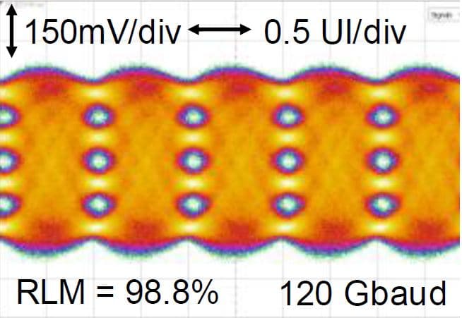
Scientists from imec-IDLab have now come up with a novel transmitter architecture that has key building blocks fabricated in a mainstream SiGe BiCMOS process. Peter Ossieur: “The resulting IC decodes 4x 30Gbaud PAM-4 (or 4x 60Gb/s NRZ) streams, and simultaneously multiplexes and equalizes these streams into a 120Gbaud PAM-4 signal with >80GHz bandwidth, 1.2Vpp voltage swing and 2200mW power consumption. Since the 4-level pulse amplitude PAM-4 modulation format involves two bits per symbol (denoted as 00, 01, 10 and 11), this is the equivalent of a 240Gb/s (single lane) transmitter.”
Key SiGe BiCMOS components in an innovative architecture
Within the transmitter IC, a multiplexer (MUX) combines multiple low-speed input signals (coming from e.g. a CPU or GPU within the datacenter) into a single full-rate data stream. This stream is subsequently equalized to compensate for any bandwidth losses in the modulator and the channel. The high-speed equalized signal is then used as an input signal for the driver that subsequently feeds the optical modulator.
In traditional transmitter architectures, equalization is performed in the digital domain, by using a digital signal processor (DSP) fabricated in advanced CMOS nodes. The equalized signal is then converted into an analog signal, feeding the driver. When high voltage swings are required, this driver is nowadays fabricated in III/V technology.
“Our innovative transmitter IC architecture implements an analog signal processing variant of the DSP filter, i.e., a 7-tap mixed-signal fast-forward equalizer (FFE) with finite impulse response (FIR) filter. Moreover, all key components, i.e., the integrated MUX, FFE and driver are fabricated in mainstream 55nm SiGe BiCMOS technology.”
A 120GBaud PAM-4 prototype
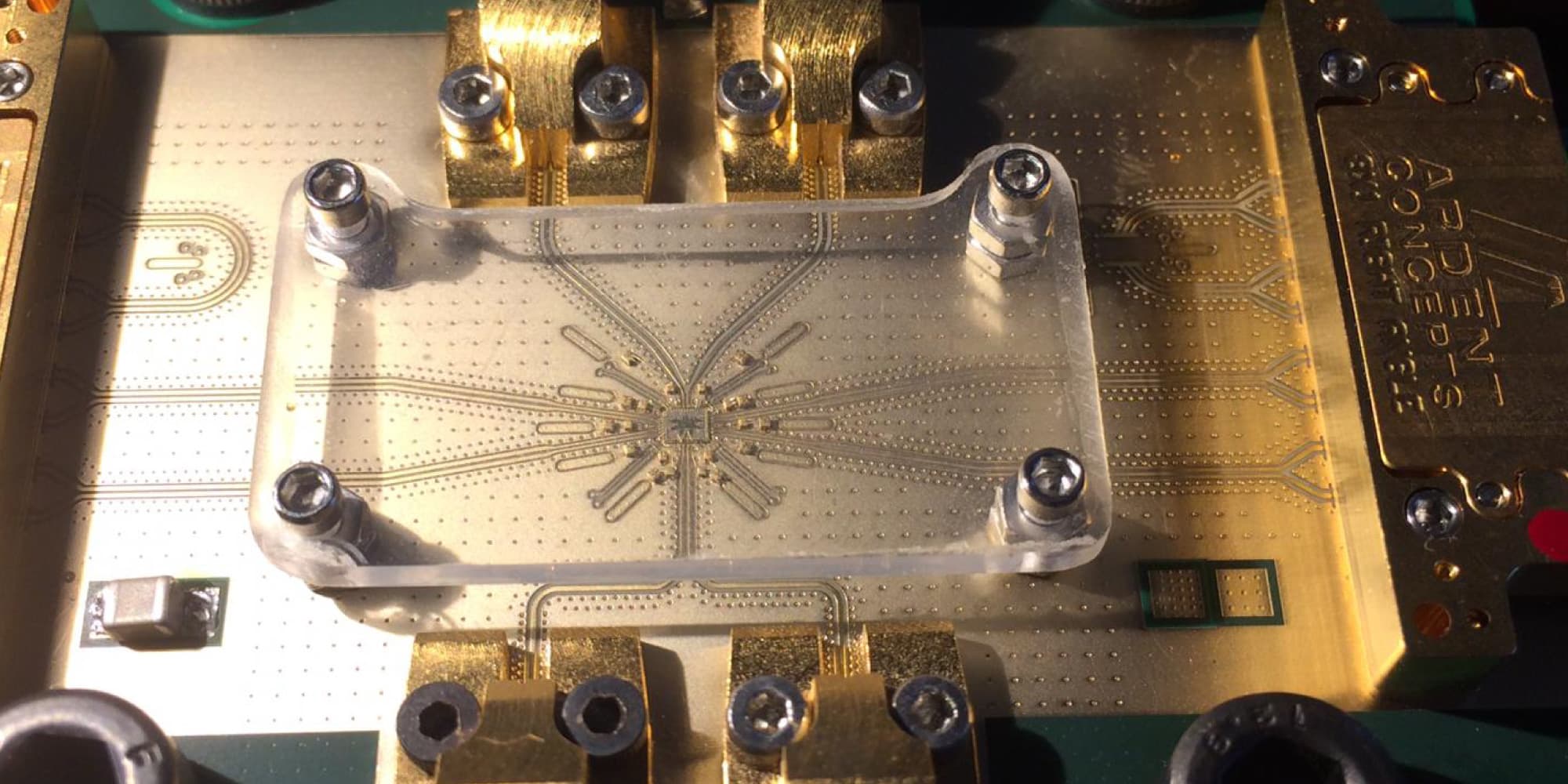
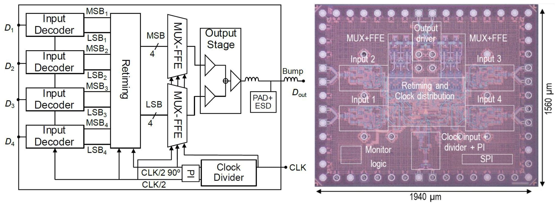
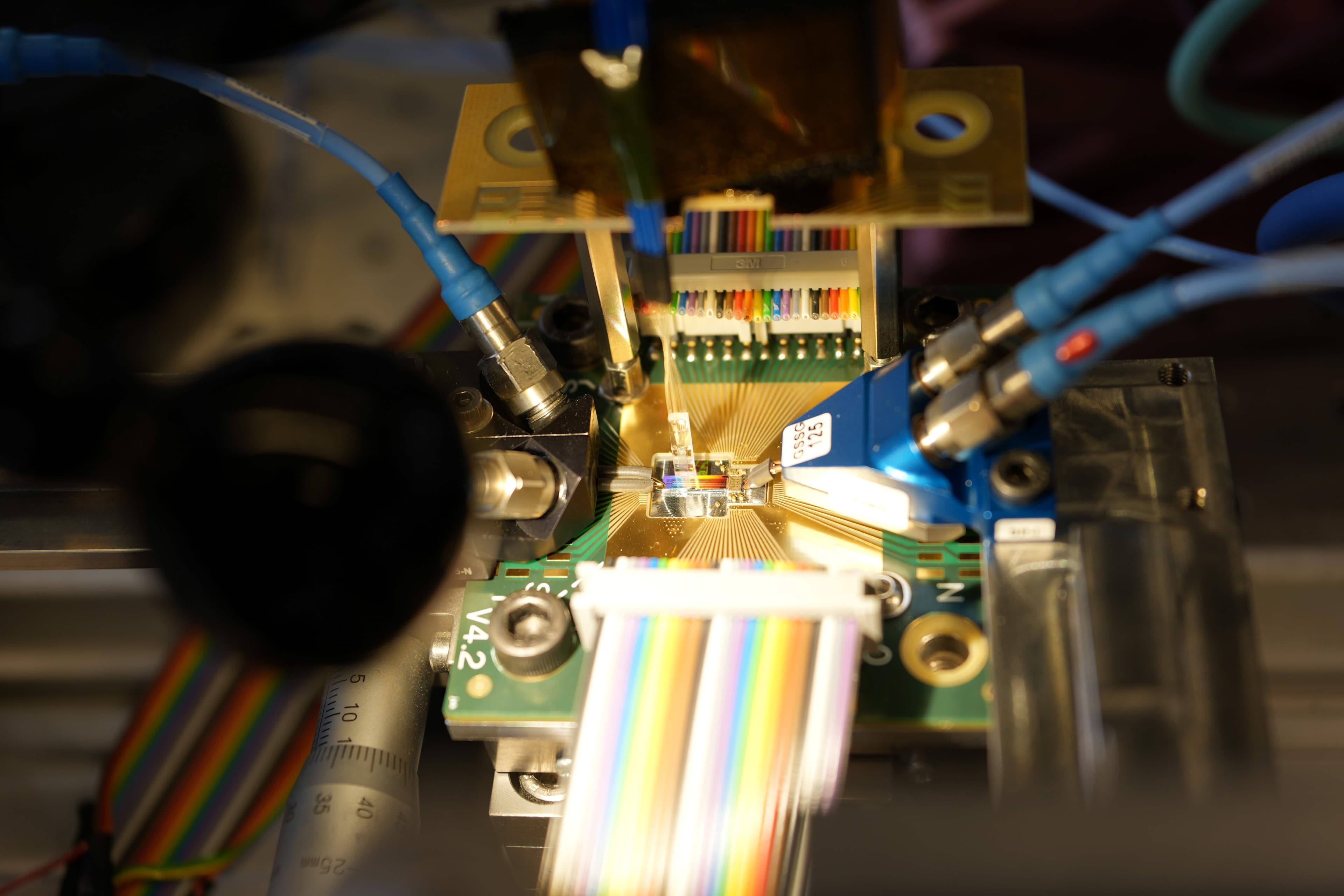
In a prototype transmitter IC, four 30 Gbaud PAM-4 input signals are processed to obtain the two components of the PAM-4 signal, i.e., the most and least significant bit (MSB and LSB) signals. The 4xMSB and 4xLSB signals are separately multiplexed and filtered by the 7-tap FFEs. The filtered signals are combined in the output stage to obtain a full-rate 120GBaud PAM-4 signal, feeding the driver. The transmitter chip is flip chipped on a high-speed PCB to allow for electrical evaluation. “The work shows a doubling of the operating rate compared to FinFET solutions and closely matches the speed and power obtained in InP-based solutions”, adds Peter Ossieur.
Future work
The >100Gbaud chips allow progression towards a new generation of optical transceivers, that can transmit these signals in either multiple fibers or at multiple wavelengths to achieve the bit rates required for the Terabit era. Apart from the building blocks described above, the team is also working on >100Gbaud transimpedance amplifiers and modulator drivers, high sampling rate ADCs and 100GSample/s analog time interleavers.
Peter Ossieur: “These building blocks will also be crucial for developing novel coherent transceiver concepts, which exploit the phase and polarization of the optical field to further increase the bit rate. The coherent transceivers target optical communication applications where low cost and low energy are critical objectives.”
This article was originally published in Electronic Design.
Want to know more?
- More details can be found in the 2021CICC paper ‘A 4-to-1 240 Gb/s PAM-4 MUX with a 7-tap Mixed-Signal FFE in 55nm BiCMOS’, from M. Verplaetse et al. Interested in receiving this paper? Fill in our contact form.
- Watch the demo movie, as presented at imec ITF Photonics 2021.
Authors

Peter Ossieur
Peter Ossieur received an M.Sc. Engineering degree in applied electronics and a Ph.D. in electrical engineering from Ghent University, Belgium, in 2000 and 2005, respectively. From 2005 to 2008, he was a Postdoctoral Fellow of the Fund of Scientific Research, Ghent University. During that time, his research was focused on 10Gbit/s burst-mode receivers and optoelectronics for automotive applications. In 2008, he became a part-time Professor of High-Frequency Electronics at the Faculty of Engineering, Ghent University.
In 2009, he joined the Photonic Systems Group, Tyndall National Institute and the Department of Physics, University College Cork, Cork, Ireland, where he became Senior Staff Researcher in April 2013. In this position he established an IC design group focusing on opto-electronic applications. In October 2017 he joined IDLab, an imec research group at Ghent University, as Senior Researcher and is currently Program Manager High-Speed Transceivers. He leads research activity focused on the development of high-speed analog and mixed-signal integrated circuits for photonic applications. He has (co-) authored 120 peer-reviewed papers, and holds several patents in the aforementioned research areas.
Discover more

Veeco and imec develop 300mm-compatible process to enable integration of barium titanate on silicon photonics
Read more
A double world-first: integrating lithium niobate and lithium tantalate modulators on silicon photonics through micro-transfer printing
Read more
Imec demonstrates the co-integration of its high-quality SiN waveguide technology with its active silicon photonics platform
Read more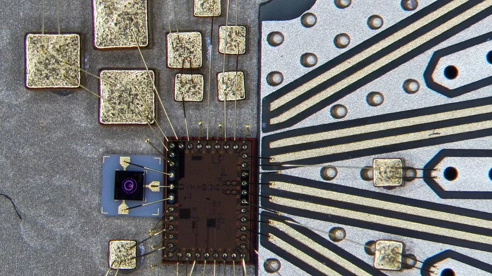
Imec researchers at Ghent University and Nokia Bell Labs work to debut key building block for the deployment of 100G PON networks
Read more
Design and integration of photonic and electronic integrated circuits for high-speed wireline transceivers
Read more