Webinar: Application-specific ICs: a unique way to customize medtech solutions

If you follow the trends in medical innovation, you know that microelectronics and silicon chip technologies are revolutionizing the medtech industry. Thereby improving the quality of healthcare and thus patients’ lives.
Application-specific ICs – so called ASICs – are a unique way to customize healthcare solutions. By reducing form factors and integrating sensing and communication features, they benefit both healthcare providers and patients. Moreover, an ASIC is an excellent way to protect your IP.
Developing an ASIC can be a complex process. That’s where you need support – whether it’s for design, development of prototype samples or volume production of qualified packaged products.
This webinar will present the latest technology trends in medtech, illustrated with ASIC examples from prototype development to commercial product.
What you will learn:
- Why is an ASIC the most disruptive technology for your medical device?
- What are the key steps?
- How can innovators get support to realize their idea in silicon?
This webinar is designed for professionals in the medtech sector who want to increase their knowledge of ASIC technologies.
About IC-Link
IC-Link is part of the global R&D hub imec, and provides complete ASIC solutions. Its services are available for customers worldwide and its teams are based in Europe, the USA, China, India, Japan, Brazil and Israel.
About the speakers
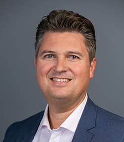
Romano Hoofman
Romano is Program Director at IC-Link since 2016. He is currently responsible for the innovation programs of the unit and for the coordination of the EUROPRACTICE Service.
He started his career in industry, where he worked as a Principal Scientist at Philips Research and later at NXP Semiconductors. He covered many different R&D topics, ranging from CMOS integration, advanced packaging, thin-film batteries, photovoltaics and (bio)sensors.
Romano received his PhD from the Technical University of Delft in 2000, where he investigated charge transport in semi-conducting polymers. He has authored more than 30 publications and holds more than 10 patents in various research areas

Paul Malisse
Paul has a master’s degree in electronics from the Politechnical Highschool Bruges-Ostend. After graduation he joined imec and has been working at IC-Link with a mission to stimulate the semiconductor ecosystem with initial focus on Europe for both industry and academia.
Paul was involved in the EUROPRACTICE service since the beginning and has held different positions throughout his career at imec. He is now leading business development team with focus on ASIC services for specific regions and applications. In his role he has very strong connections with - and understanding of the foundry ecosystem.
Complete this form to register
Note that if you have an ad blocker, you may not see the registration form below. Disable ad blockers to register.
Discover more