Machine learning accelerators
Edge AI systems will need to make split-second decisions using a tiny amount of energy. Imec is working on the hardware optimizations to enable the needed leap in efficiency.
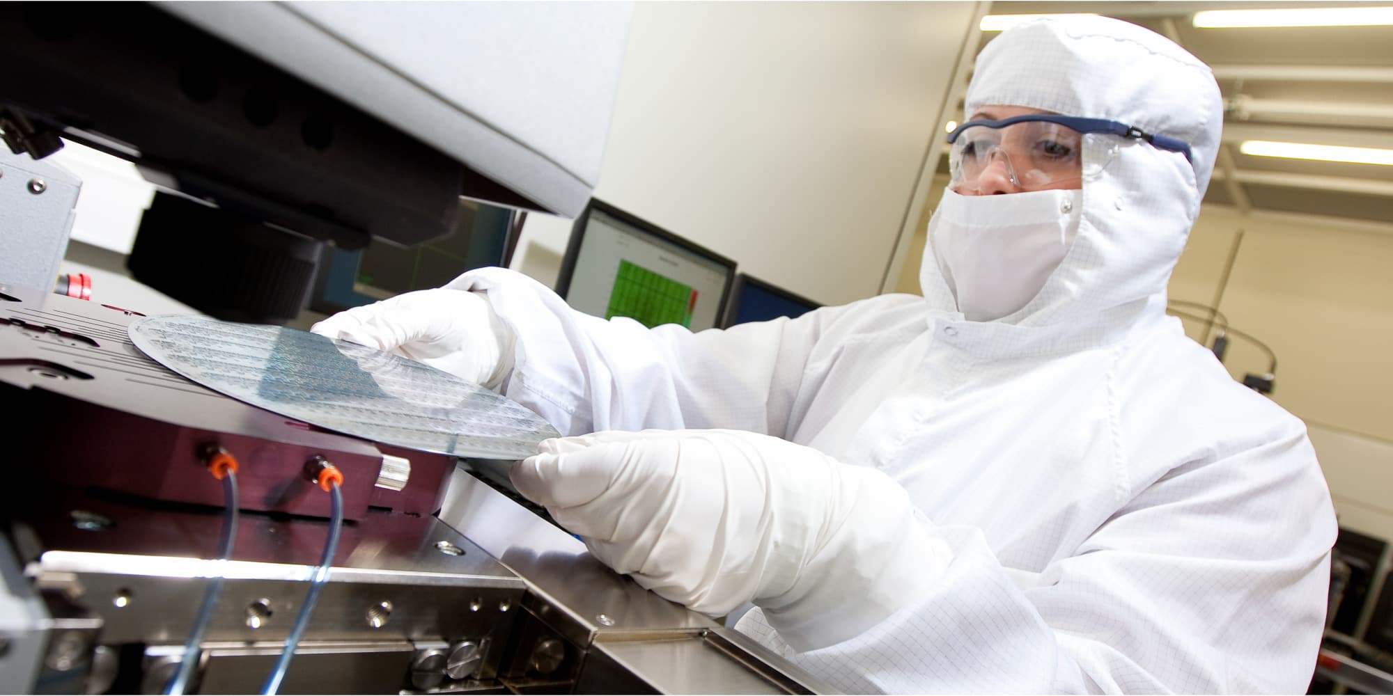
For AI computing, shuttling data from where they are generated to a data center takes time and bandwidth that are not always available. Think edge devices that run on batteries. Or an autonomous vehicle that needs to make near instantaneous decisions based on AI.
Today, commercially available edge AI ICs – the chips inside the servers at the edge of networks – offer efficiencies in the order of 1-100 tera operations per second per Watt (tops/W), using fast GPUs or ASICs for computation.
But for most IoT implementations (smartphones, body sensors…), much higher efficiencies will be needed. Imec’s goal is therefore to demonstrate efficiencies for machine learning inference in the order of 10,000 Tops/W.

Read this article about why and how to tackle the energy costs of AI.
Accelerating machine learning with compute-in-memory
To address this challenge, imec and its partners have set up a research program to build innovative machine learning accelerators. The core idea is to look beyond the Von Neumann paradigm, the conventional design in which processors and memory are separated.
This proves especially cumbersome in neural networks, which depend on large vector matrix multiplications. The many required reads and writes to the separate memory cost much more energy than the computing itself.
The program’s aim is therefore to work with compute-in-memory architectures. In such processors, the computation is performed inside a memory framework, saving most of the power otherwise needed to move data back and forth. Also, with the analog approach, the required multiplications can be performed at lower but sufficient precision than in a digital core, again saving time and energy.
AnIA: a novel AI IC
In 2020, we demonstrated such an Analog Inference Accelerator (AnIA) with an exceptional energy efficiency. Tests showed it to reach 2,900 Tops/W for vector matrix multiplications. This would make it suitable for local pattern recognition in tiny sensors and low-power edge devices, which are now typically powered by machine learning in data centers.
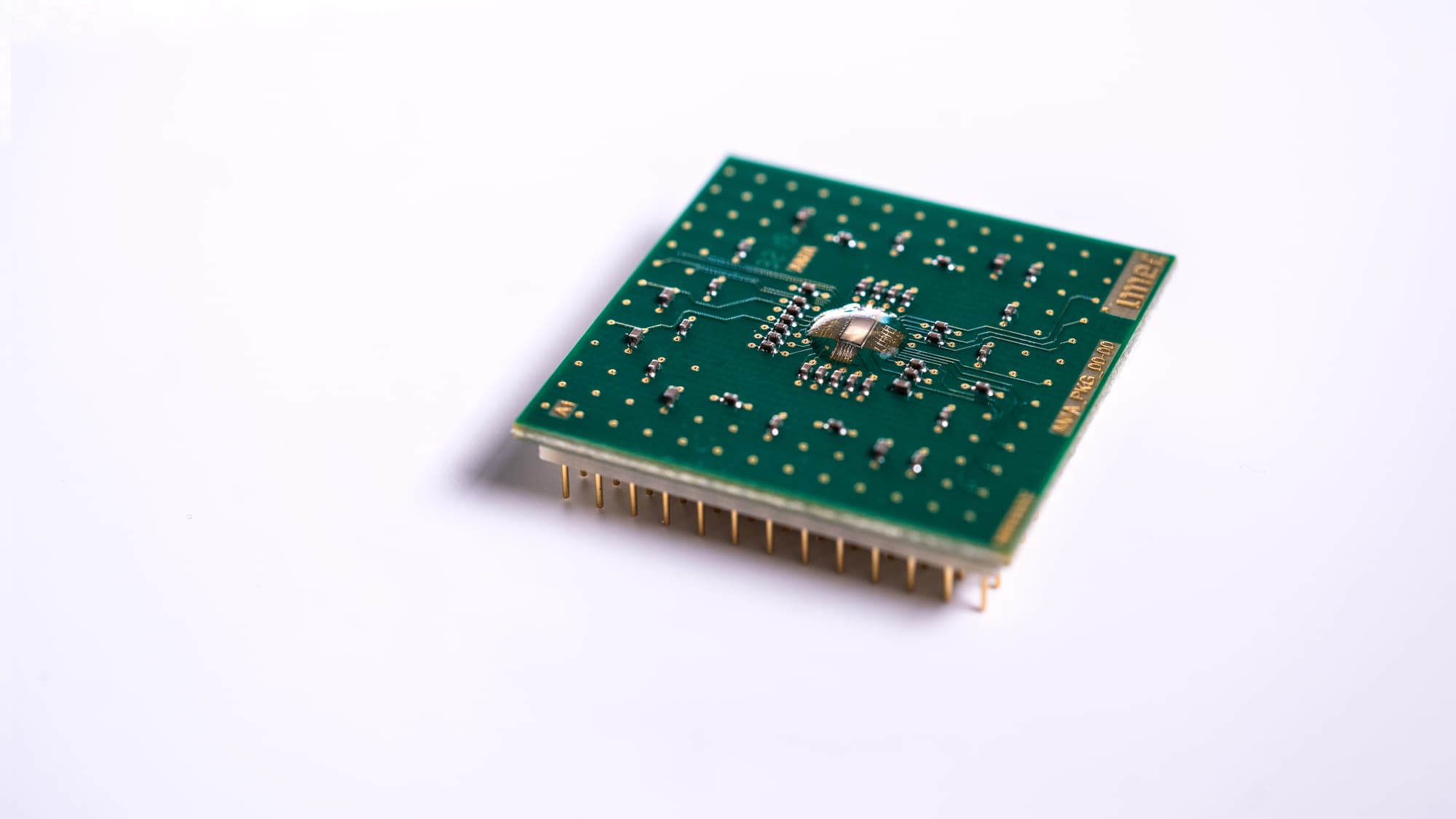
This successful tape-out marks an important step forward toward validation of Analog in Memory Computing (AiMC). It not only shows that analog in-memory calculations are possible in practice, but also that they achieve an energy efficiency ten to hundred times better than digital accelerators. To further improve this number towards 10,000Tops/W, imec and partners are researching non-volatile memories such as SOT-MRAM, FeFET and IGZO-based memories.
Imec not only helps you to address technological challenges. Thanks to our thorough knowledge of the industry, we function as your full-fledged strategic partner – right down to venturing support.
Click the button below to get in touch.
Read more
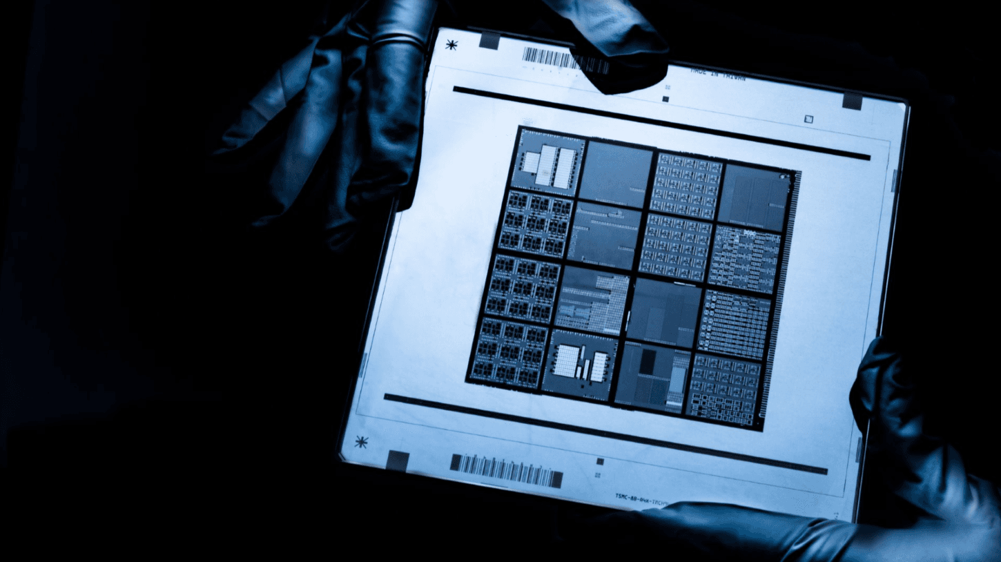
When does it make sense to move from a monolithic ASIC to a chiplet-based design?
A journey into the benefits, trade-offs and technical implications of moving to chiplets
Read more
Cross-technology co-optimization (XTCO)
A holistic approach to system scaling, connecting AI workload challenges to technology innovations.
Read more
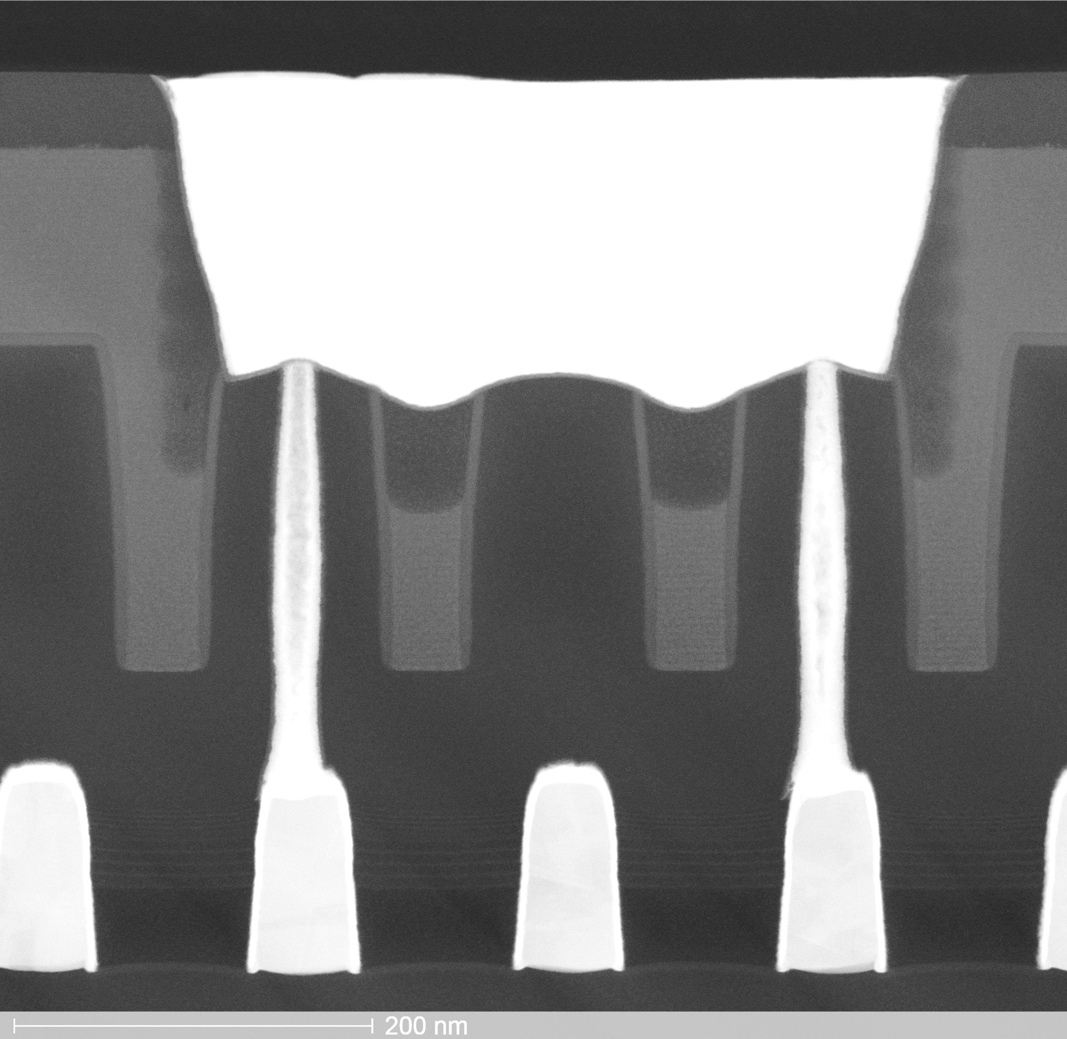
Sony and imec unveil high-density backside connectivity module enabling next-generation 3D chip integration
The new integration approach implements sub-100nm self-aligned through-Si via connections, enabling low-resistance and low-leakage front-to-back connections with good overlay performance
Read more