Imec’s extremely scaled SOT-MRAM devices show record low switching energy and virtually unlimited endurance
Scaling the spin-orbit transfer (SOT) track as a critical step towards SOT-MRAM for cache memory applications

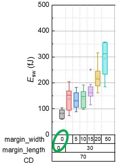
LEUVEN (Belgium), December 13, 2023— This week, at the 2023 International Electron Devices Meeting (IEEE IEDM 2023), imec, a world-leading research and innovation hub in nanoelectronics and digital technologies, presents extremely scaled spin-orbit transfer magnetic random-access memory (SOT-MRAM) devices showing the best published performance ever. Achieving a switching energy below 100 femto-Joule per bit and >1015 endurance, these breakthrough results bring non-volatile SOT-MRAM technology a step closer to last-level cache memory applications.
SOT-MRAM is a promising candidate for replacing SRAM as a last-level cache memory in high-performance computing (HPC) applications. Just like SRAM, it offers a high switching speed (in the sub-ns regime) and promises unlimited endurance. Moreover, being nonvolatile, SOT-MRAM bit cells achieve lower standby power than SRAMs at high cell density. Also, SOT-MRAM bit cells can potentially be made much smaller than SRAM cells, translating into a higher bit packing density.
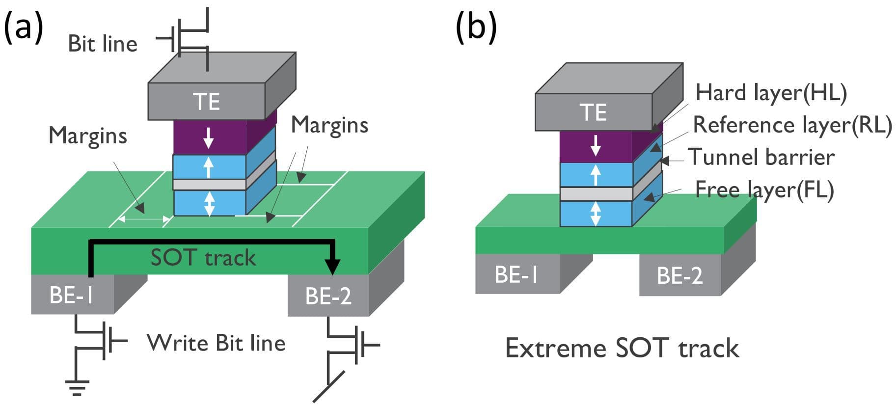
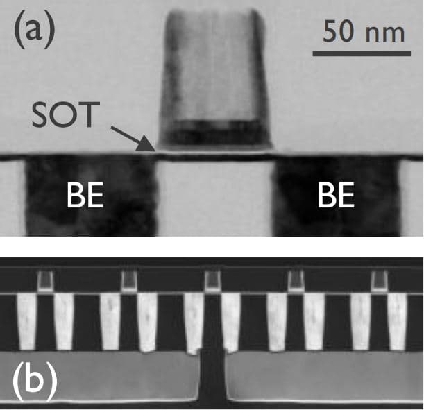
Imec has experimentally explored the scaling potential and limitations of single perpendicular SOT-MRAM devices processed on 300mm wafers – the first ever reported study on SOT-MRAM device scalability. At IEDM 2023, they show that scaling the SOT track not only reduces the footprint of the SOT-MRAM cell, but also largely improves the cell’s performance and reliability.
The SOT track is a layer made of metal such as tungsten (W) or platinum (Pt) that resides below the magnetic tunnel junction (MTJ) – the actual switching element of the SOT-MRAM device. The SOT track serves as an in-plane current injection layer, which has been introduced to de-couple read and write paths. “In conventional SOT-MRAM designs, the area occupied by the SOT track is larger than the actual MTJ pillar footprint to provide sufficient margin for overlay process control,” explains Sebastien Couet, program director magnetics at imec. “But this results in wasted energy, as part of the current flows outside the MTJ area. We scaled SOT-MRAM devices to their extreme, with SOT track and MTJ pillar having comparable dimensions (critical dimension ~50nm). For these devices, we observed a switching energy below 100 femto-Joule (fJ) per bit, i.e., a reduction of 63% compared to conventional designs. This helps address a remaining challenge of SOT-MRAM, which traditionally requires a high current for the write operation.”
On top of that, we showed that scaling the SOT track improves the memory’s endurance, as it reduces Joule heating inside the SOT layer. Sebastien Couet: “With an endurance beyond 1015 program/erase cycles, we have experimentally validated our assumption that SOT-MRAM cells can have unlimited endurance – an important requirement for cache memories.”
“Our data provide valuable input for circuit designers to perform design-technology co-optimization (DTCO) of SOT-MRAM technology at advanced nodes – trading of performance improvement and design margins. Future work focuses on material engineering to further reduce the switching energy per bit, and on optimizing bit cell configuration to further shrink the cell area compared to SRAM. On the longer term, these learnings will also be transferred to the development of voltage-gated (VG) SOT-MRAM multi-pillar devices – imec’s ultimate solution for high-density embedded memory applications,” adds Sebastien Couet.
About imec
Imec is a world-leading research and innovation center in nanoelectronics and digital technologies. Imec leverages its state-of-the-art R&D infrastructure and its team of more than 5,500 employees and top researchers, for R&D in advanced semiconductor and system scaling, silicon photonics, artificial intelligence, beyond 5G communications and sensing technologies, and in application domains such as health and life sciences, mobility, industry 4.0, agrofood, smart cities, sustainable energy, education, … Imec unites world-industry leaders across the semiconductor value chain, Flanders-based and international tech, pharma, medical and ICT companies, start-ups, and academia and knowledge centers. Imec is headquartered in Leuven (Belgium), and has research sites across Belgium, in the Netherlands and the USA, and representation in 3 continents. In 2022, imec's revenue (P&L) totaled 846 million euro.
Further information on imec can be found at www.imec-int.com.
Imec is a registered trademark for the activities of imec International (IMEC International, a legal entity set up under Belgian law as a “stichting van openbaar nut”), imec Belgium (IMEC vzw supported by the Flemish Government), imec the Netherlands (Stichting IMEC Nederland), imec Taiwan (IMEC Taiwan Co.), imec China (IMEC Microelectronics (Shanghai) Co. Ltd.), imec India (IMEC India Private Limited), imec San Francisco (IMEC Inc.) and imec Florida (IMEC USA Nanoelectronics Design Center Inc.).
Discover more
Imec achieves breakthroughs in ferroelectric memory research for next-generation memory solutions to meet AI-era data needs
Read more

Imec demonstrates the first 3D implementation of a charge coupled device for AI memory applications
Read more