Imec proposes double-row CFET for the A7 technology node
New standard cell architecture offers the most optimal trade-off between area efficiency and process complexity for logic and SRAM.
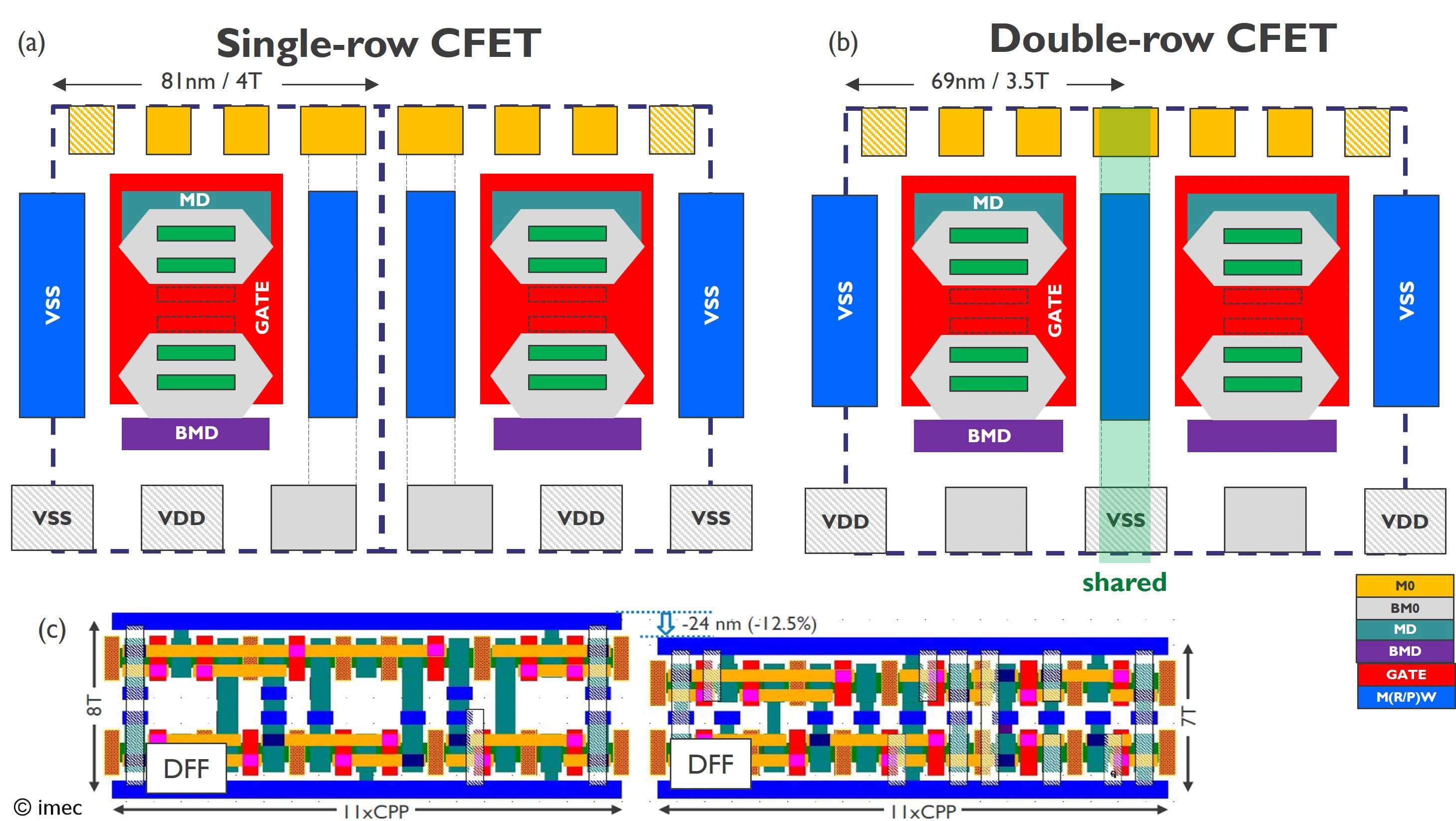
LEUVEN (Belgium), December 7, 2024— This week, at the 2024 IEEE International Electron Devices Meeting (IEDM), imec, a world-leading research and innovation hub in nanoelectronics and digital technologies, presents a new CFET-based standard cell architecture containing two rows of CFETs with a shared signal routing wall in between. The main benefits of this double-row CFET architecture are process simplification, and significant logic and SRAM cell area reduction according to imec’s design-technology co-optimization (DTCO) study. The new architecture allows standard cell heights to be reduced from 4 to 3.5T, compared to conventional single-row CFETs.
The semiconductor industry is making considerable progress in fabricating (monolithic) CFET devices that are envisioned to succeed gate-all-around nanosheets (NSHs) in the logic technology roadmap. The stacking of n- and pFET devices promises benefits in power, performance, and area (PPA) when combined with backside technologies for power delivery and signal routing. At the circuit level, however, several options are still open for integrating the CFETs into a standard cell to sustain or enhance the expected PPA benefits. Especially challenging is the middle-of-line (MOL) connectivity, i.e., the interconnects that connect source/drain and gate contacts to the first metal lines (at back- and frontside) and ensure top-to-bottom connectivity for both power and signal.
From a DTCO study comparing standard cell architectures, imec shows that the double-row CFET offers the most optimal trade-off between manufacturability and area efficiency for A7 logic nodes. This new architecture starts from a base cell in which one side of the CFET is optimized for power connections – including a power rail (VSS) to deliver power from the backside to the top device and a direct backside connection for the bottom device. The other side is optimized for signal connections by providing a middle routing wall (MRW) for top-to-bottom connectivity. The double-row CFET standard cell (with two rows of stacked devices) is then formed by mirroring two base cells, which share the same MRW for signal connectivity (see Figure 1).
Geert Hellings, Program Director DTCO at imec: “Our DTCO study shows that one shared MRW for every 3.7 FET is sufficient to build logic and SRAM cells. This allows us to further reduce standard cell heights from 4 to 3.5T, compared to ‘classical’ single-row CFETs. This translates into a significant area reduction of 15 percent for SRAM cells. Compared to SRAMs built with, e.g., A14 NSH technology, double-row CFET-based SRAMs enable more than 40 percent area shrinkage, providing a further scaling path for SRAMs.” The double-row CFET also leads to process simplification because of the shared MRW trench between two rows of CFET devices. This eliminates the need for an extra high-aspect-ratio via to connect the top and bottom devices, if necessary, reducing MOL processing complexity and cost.
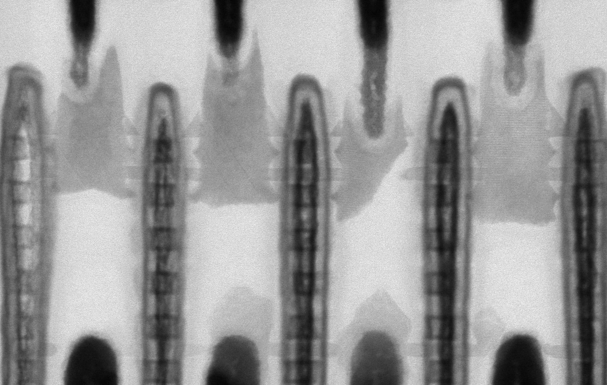
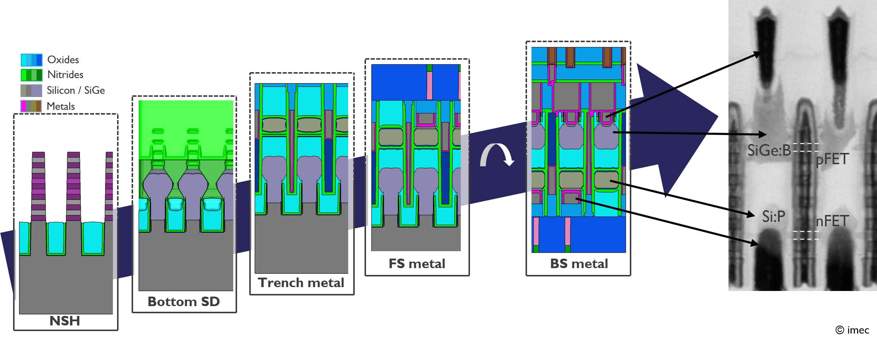
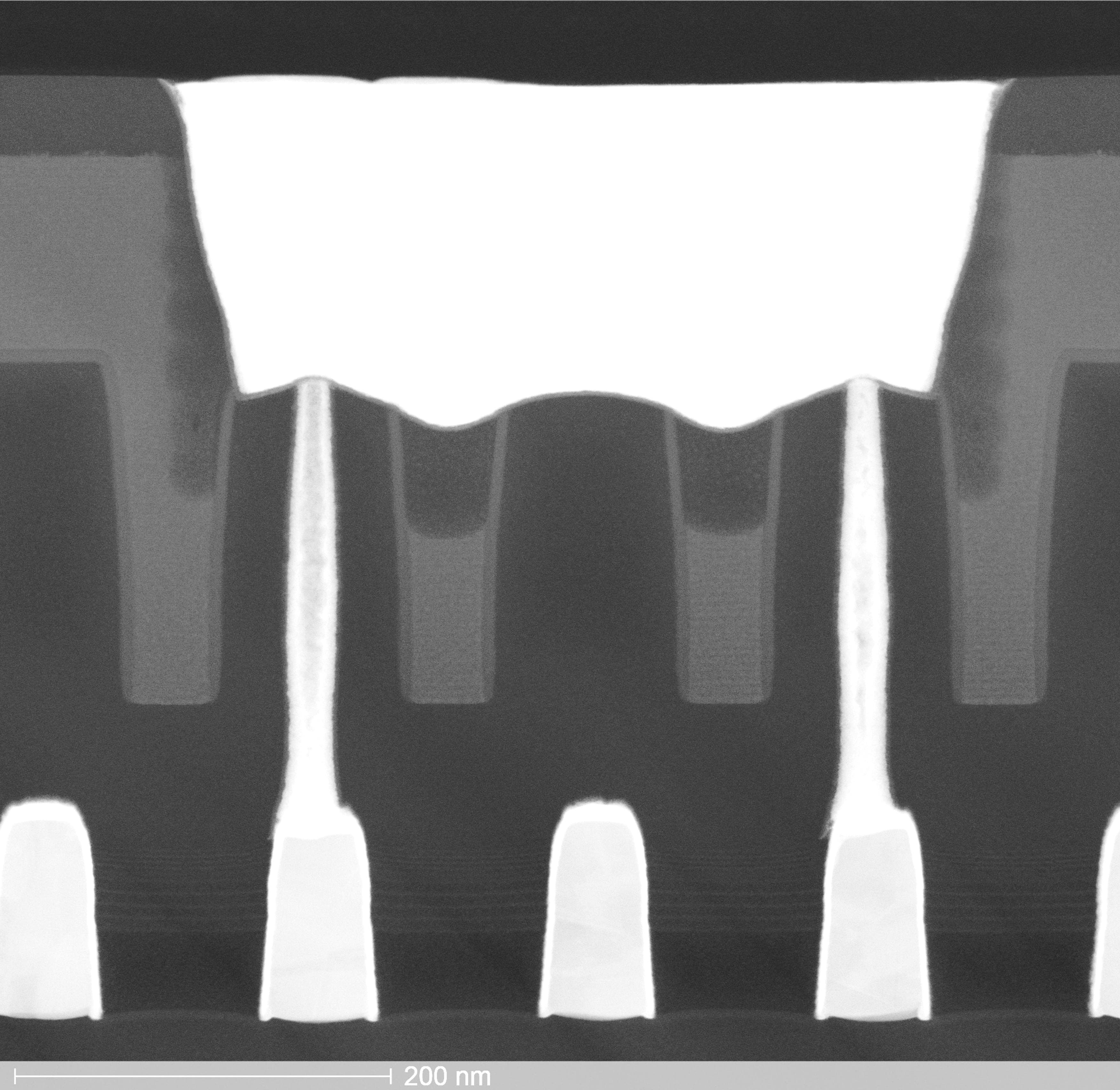
“Since the 7nm technology node, standard cell optimization through DTCO is providing an increasingly large share of node-to-node density increase, in addition to conventional device scaling,” adds Geert Hellings. “For our DTCO study on CFET architectures, we started from the process capabilities envisioned in future CFET fabs to ensure industry-relevant process flows (Figure 2). In addition, we validate our virtual fab concept with technology proofs-of-concept performed in imec’s 300mm cleanroom. This combination of virtual fab and real pilot line activities is a crucial step in advancing our roadmaps.” As such, also at IEDM, imec experimentally demonstrated a key building block of this double-row CFET architecture: a functional monolithic CFET with direct backside contact to the source/drain of the bottom pMOS device. This was realized through EUV backside patterning that ensured dense backside power and signal wiring and tight overlay (<3nm accuracy) between the source/drain created from the frontside, backside contact, and subsequent backside metal layers (Figure 2).
About imec
Imec is a world-leading research and innovation center in nanoelectronics and digital technologies. Imec leverages its state-of-the-art R&D infrastructure and its team of more than 5,500 employees and top researchers, for R&D in advanced semiconductor and system scaling, silicon photonics, artificial intelligence, beyond 5G communications and sensing technologies, and in application domains such as health and life sciences, mobility, industry 4.0, agrofood, smart cities, sustainable energy, education, … Imec unites world-industry leaders across the semiconductor value chain, Flanders-based and international tech, pharma, medical and ICT companies, start-ups, and academia and knowledge centers. Imec is headquartered in Leuven (Belgium), and has research sites across Belgium, in the Netherlands, the UK and the USA, and representation in 3 continents. In 2023, imec's revenue (P&L) totaled 941 million euro.
Further information on imec can be found at www.imec-int.com.
Imec is a registered trademark for the activities of imec International and its affiliated entities.
Discover more


Sony and imec unveil high-density backside connectivity module enabling next-generation 3D chip integration
Read more

ASML, TSMC and imec bring industry-ready 2D-material transistors closer with breakthrough 300mm integration
Read more