Imec proposes 3D charge-coupled device with IGZO channel as buffer memory for data-intensive compute applications
The new compute express link (CXL) type-3 buffer memory promises to vastly surpass DRAM in terms of bit density and cost efficiency
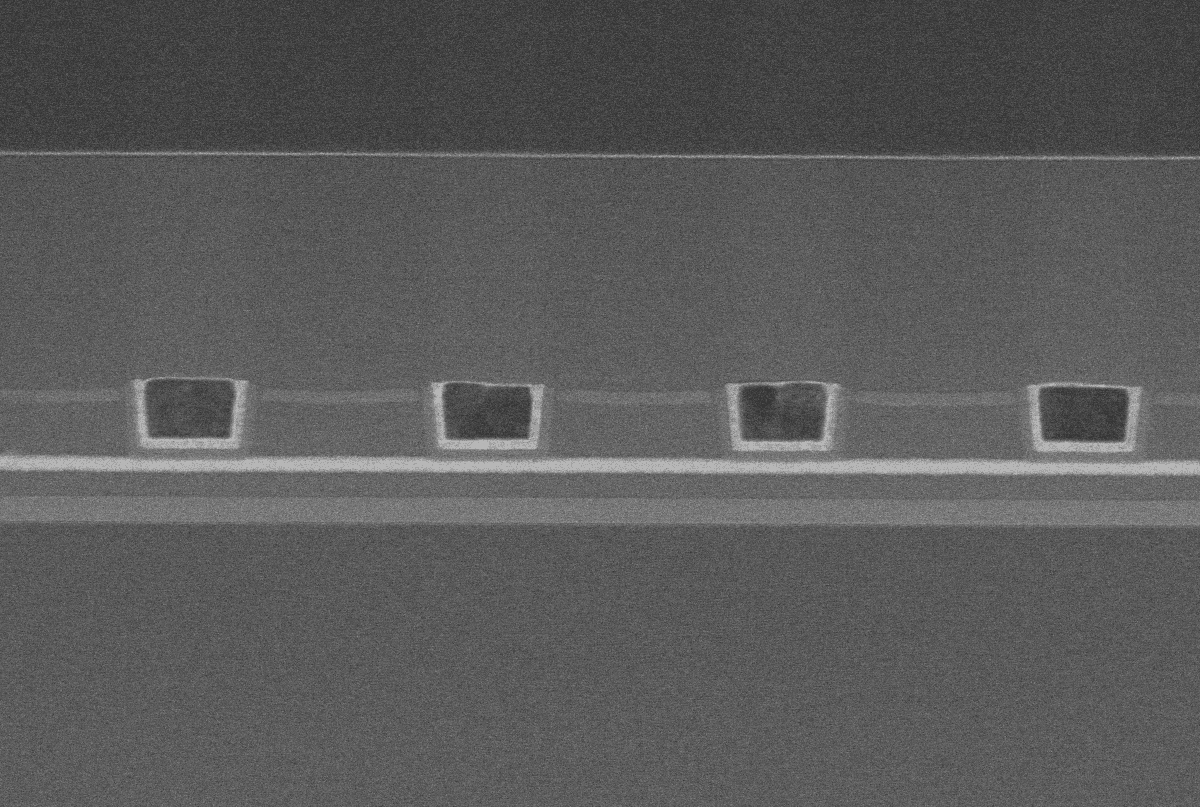
LEUVEN (Belgium), December 12, 2024— This week, at the 2024 IEEE International Electron Devices Meeting (IEDM), imec, a world-leading research and innovation hub in nanoelectronics and digital technologies, proposes a novel 3D integrated charge-coupled device (CCD) that can operate as a block-addressable buffer memory, in support of data-intensive compute applications. Memory operation is demonstrated on a planar proof-of-concept CCD structure which can store 142 bits. Implementing an oxide semiconductor channel material (such as IGZO) ensures sufficiently long retention time and enables 3D integration in a cost-efficient, 3D NAND-like architecture. Imec expects the 3D CCD memory density to scale far beyond the DRAM limit.
The recent introduction of the compute express link (CXL) memory interface provides opportunities for new memories to complement DRAM in data-intensive compute applications like AI and ML. One example is the CXL type-3 buffer memory, envisioned as an off-chip pool of memories that ‘feeds’ the various processor cores with large data blocks via a high-bandwidth CXL switch. This class of memories meets different specifications than byte-addressable DRAM, which increasingly struggles to maintain the cost-per-bit-trend scaling line.
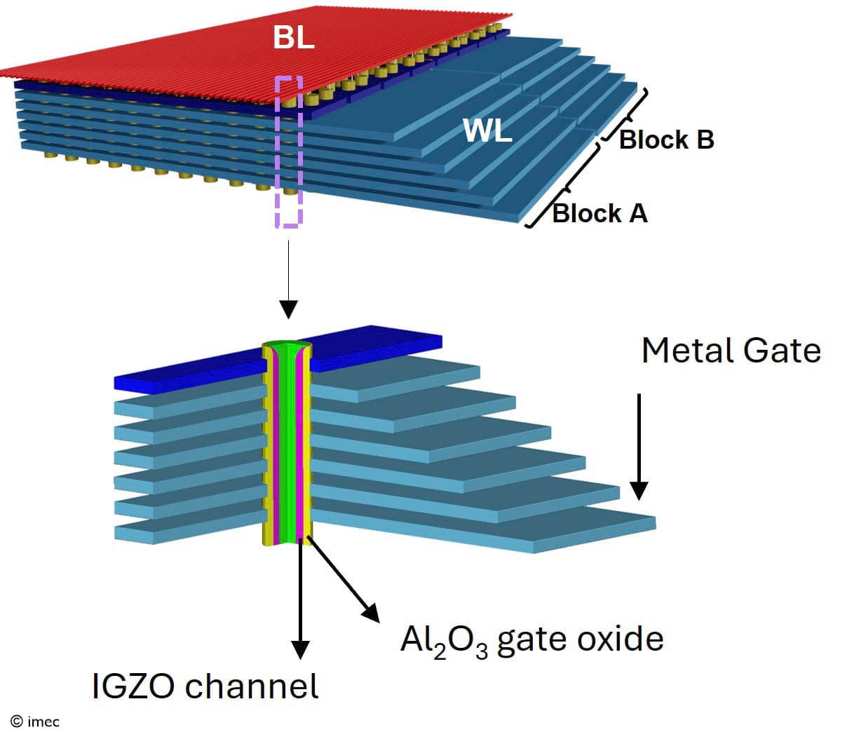
At IEDM 2024, imec proposes a charge-coupled device (CCD) with IGZO channel integrated into a 3D NAND-Flash string architecture as a promising candidate for CXL type-3 buffer memory – to achieve the required characteristics of block addressability, unlimited endurance, low fabrication cost, and sufficient data retention.
As a first step towards real implementations, imec demonstrated memory operation of the CCD with IGZO on a 2D proof-of-concept. The planar CCD structure of this 2D proof-of-concept consists of an input stage, 142 stages (each consisting of four phase gates) which can each store one bit, and a two-transistor-based read-out stage. The CCD register is written by injecting charges through the input stage and sequentially transferring them through all 142 stages by switching the voltages of the phase gates. The CCD offers more than 200s retention, an endurance of >1010 cycles without degradation, and a charge transfer speed exceeding 6MHz. Multilevel storage capability of the CCD register was also demonstrated, contributing to a higher bit density. Being widely adopted in the image sensor market, the charge-based CCD technology is well-known, reliable, and can operate at low voltages – benefiting power consumption.
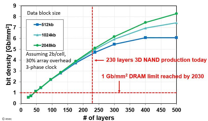
Maarten Rosmeulen, Program Director Storage Memory at imec: “The real value of the proposed buffer memory lies in its ability to be integrated into 3D NAND fashion, with IGZO-based CCD registers integrated into vertically aligned plugs – a concept that we now propose for the first time. From what is possible with NAND Flash today (i.e., the capability of processing 230 layers), we estimate that our 3D buffer memory can already provide five times more bit density than what (2D) DRAM is expected to offer in 2030. We are currently investigating real 3D implementations with limited number of word lines.”
About imec
Imec is a world-leading research and innovation center in nanoelectronics and digital technologies. Imec leverages its state-of-the-art R&D infrastructure and its team of more than 5,500 employees and top researchers, for R&D in advanced semiconductor and system scaling, silicon photonics, artificial intelligence, beyond 5G communications and sensing technologies, and in application domains such as health and life sciences, mobility, industry 4.0, agrofood, smart cities, sustainable energy, education, … Imec unites world-industry leaders across the semiconductor value chain, Flanders-based and international tech, pharma, medical and ICT companies, start-ups, and academia and knowledge centers. Imec is headquartered in Leuven (Belgium), and has research sites across Belgium, in the Netherlands, the UK and the USA, and representation in 3 continents. In 2023, imec's revenue (P&L) totaled 941 million euro.
Further information on imec can be found at www.imec-int.com.
Imec is a registered trademark for the activities of imec International and its affiliated entities.
Discover more

Imec achieves breakthroughs in ferroelectric memory research for next-generation memory solutions to meet AI-era data needs
Read more

Imec demonstrates the first 3D implementation of a charge coupled device for AI memory applications
Read more