Imec Applies Photolithography To Push Functionality and Reliability Barriers In OLED Display Manufacturing
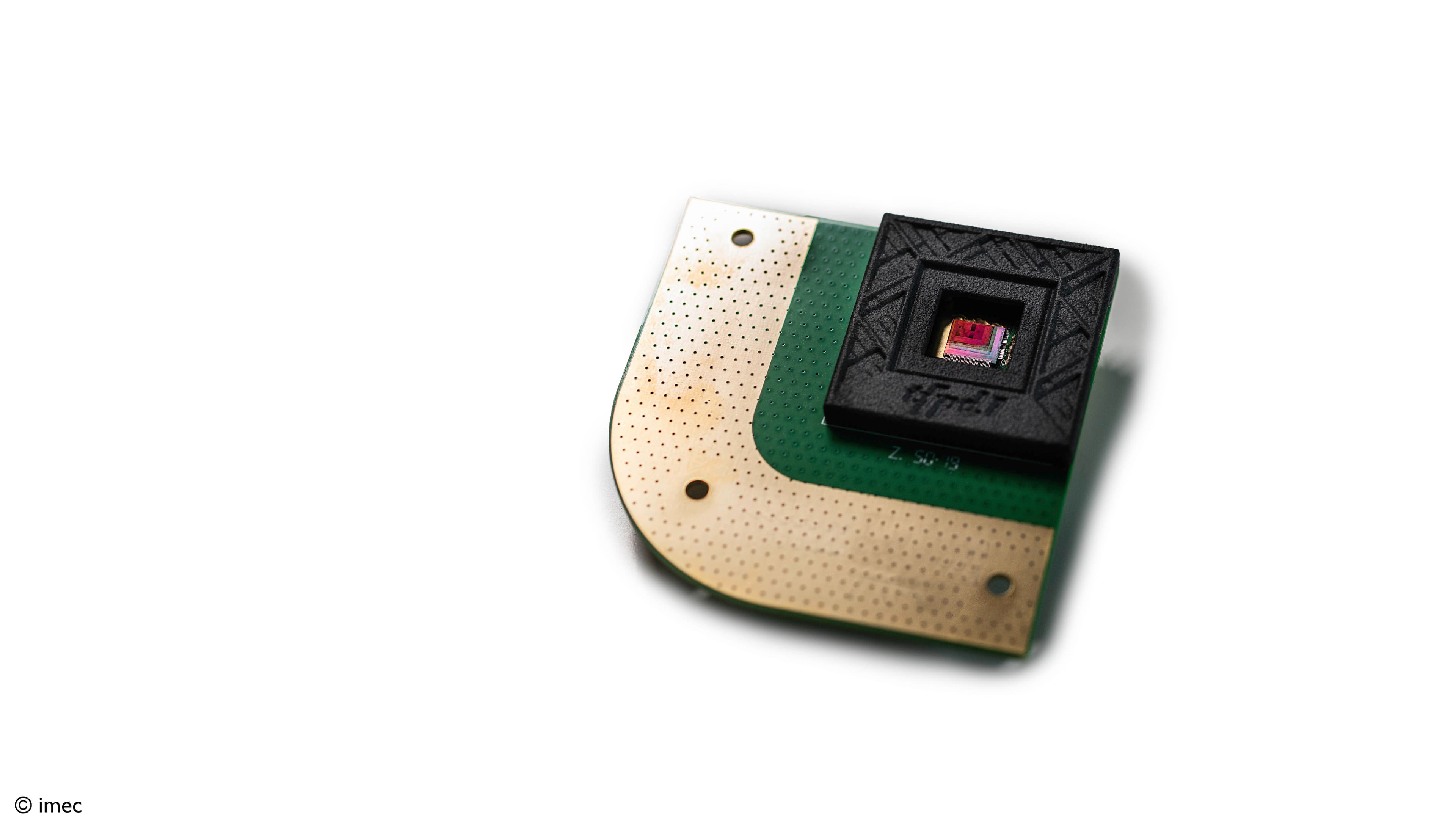
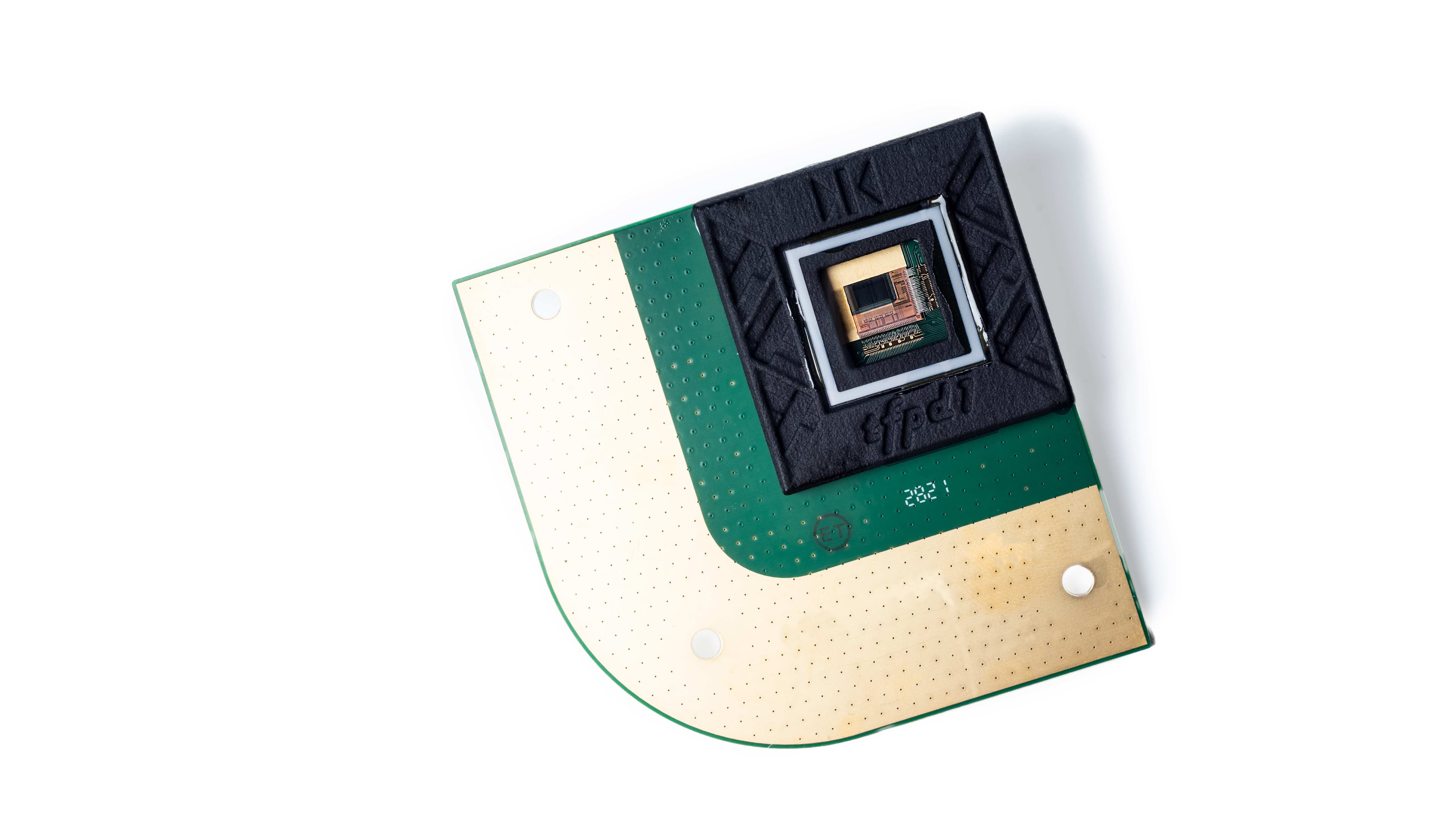
LEUVEN (Belgium), 3 December, 2020 — Next week, at the International Display Workshop 2020, imec, a world-leading research and innovation hub in nanoelectronics and digital technologies, presents the application of photolithography to pattern organic semiconductors and the cathode in an OLED-display stack with a breakthrough device reliability and which has the potential to eliminate the use of fine metal masks (FMM). The demonstration is important for display manufacturers as photolithography enables higher resolutions or an increased transparency of the cathode to accommodate for display-integrated sensors. Imec is open for collaboration with industrial partners on this topic and can offer design-on-demand services related to this result.
In the domain of mobile displays, the demand to increase the screen-to-body ratio pushes manufacturers to enable new form factors and hide an increasing amount of functionality (e.g. front-side camera, fingerprint sensor…) inside the screen without degrading the image quality. But also in high-end mobile, TV and pc/laptop applications, manufacturers are craving for active-matrix OLED (AMOLED) screens to offer unique properties such as vivid colors and flexible and ultrathin format to enable the innovative form factors of future product designs.
At present, the use of fine metal masks (FMM) is the dominant manufacturing route to create red, green and blue light-emitting-layer (EML) patterns in AMOLED displays. Alternatively, multiple companies have shown AMOLED displays surpassing 150ppi resolution via the alternative of solution-printing processes such as inkjet printing (IJP). Yet, the use of FMM does not apply to very large area glass substrates, and IJP results in lower reliability compared to evaporated OLEDs.
By using photolithography processes, imec now provides an alternative manufacturing route that allows for higher design freedom and shows promising results in terms of reliability. For example, imec is capable of creating patterns on top of organic semiconductors with 1µm pitch (line and space), which corresponds to resolutions around 12000ppi. Also, the transparency of the OLED frontplane at higher wavelengths increased from 20 to 70% after cathode patterning. Most importantly, the results of the reliability testing show T95>200hours and no measurable difference in OLED lifetime at 1000 nits for patterned OLEDs compared to reference un-patterned OLEDs.
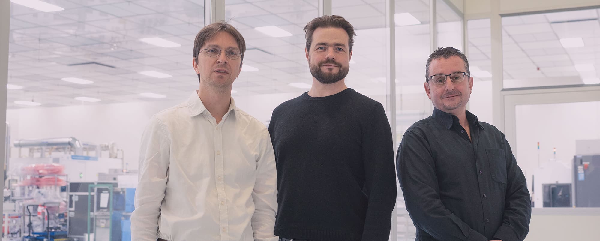
Tung Huei Ke, R&D project leader for sensor technology, at imec: “Photolithographic patterning of OLED was extremely challenging because of the chemical incompatibility of the photolithography chemistry to the OLED materials. Also, the sensitivity of OLED materials to water and oxygen in a conventional photolithography environment was a major difficulty. As the first OLED subpixel needs to be patterned at least three times to realize full-color AMOLED array, it was considered that the degradation after multiple photolithographic patterning steps would accumulate. This assumption, confirmed by earlier experiments, discouraged the industry to go for this route. Imec now shows excellent OLED reliability after multiple patterning steps by photolithography. This is an important milestone to bring photolithography as patterning technology for OLEDs to the next level. We continue working with the industrial partners to mature the technology for high-volume production and invite interested display manufacturing companies to join this endeavor.”
About imec
Imec is a world-leading research and innovation hub in nanoelectronics and digital technologies. The combination of our widely acclaimed leadership in microchip technology and profound software and ICT expertise is what makes us unique. By leveraging our world-class infrastructure and local and global ecosystem of partners across a multitude of industries, we create groundbreaking innovation in application domains such as healthcare, smart cities and mobility, logistics and manufacturing, energy and education.
As a trusted partner for companies, start-ups and universities we bring together more than 4,000 brilliant minds from over 97 nationalities. Imec is headquartered in Leuven, Belgium and has distributed R&D groups at a number of Flemish universities, in the Netherlands, Taiwan, USA, and offices in China, India and Japan. In 2018, imec's revenue (P&L) totaled 583 million euro. Further information on imec can be found at www.imec-int.com.
Imec is a registered trademark for the activities of IMEC International (a legal entity set up under Belgian law as a "stichting van openbaar nut”), imec Belgium (IMEC vzw supported by the Government of Flanders), imec the Netherlands (Stichting IMEC Nederland, part of Holst Centre which is supported by the Dutch Government), imec Taiwan (IMEC Taiwan Co.), imec China (IMEC Microelectronics (Shanghai) Co. Ltd.), imec India (Imec India Private Limited) and imec Florida (IMEC USA nanoelectronics design center).
Discover more

Swave, a new Imec and VUB, Spin-off, Raises €7M to Deliver Truly Realistic AR/VR Experiences to Applications Like the Metaverse
Read more
Imec, TNO and Cartamundi develop flexible tags that communicate with standard touch screens
Read more