Imec and Bühler Group’s Leybold Optics enable high-throughput manufacturing of filter-on-chip CMOS sensors with unmatched precision
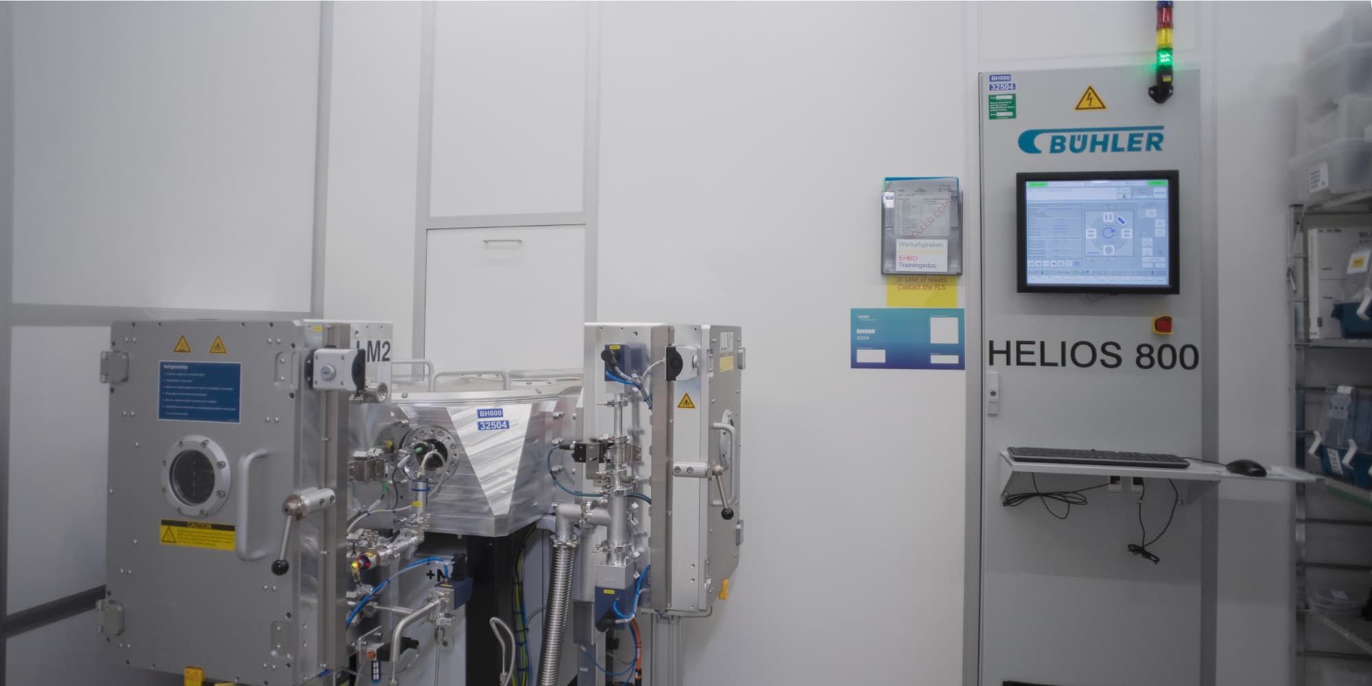
LEUVEN (Belgium) and ALZENAU (Germany), April 4, 2022 – Bühler Group’s Leybold Optics Business Area, a supplier of cutting-edge thin-film vacuum coaters, and imec, a world-leading research and innovation center in nanoelectronics, announce that they have qualified Bühler’s HELIOS 800 tool to meet the stringent standards of the semiconductor industry and developed high-performance filters for optical image sensors. The enhanced tool opens many new applications that require a precise deposition of high-quality optical stacks at high manufacturing speed. The development is going to lead to a new generation of high-resolution low-cost hyperspectral imaging sensors.
The production of high-resolution low-cost filter-on-chip CMOS detectors for hyperspectral imaging sensors (HSI) for the visible (VIS) and the short-wave infrared (SWIR) range places high demands on thin-film deposition tools. A superior optical performance and low defect levels of the interference filters, combined with maximized wafer throughputs is needed. However, state-of-the-art deposition tools in semiconductor foundries lack a sufficient coating uniformity and optical performance as well as an in-situ thickness control. In the absence of such in-situ layer thickness control, the optical properties of filter stacks with up to hundreds of layers would need to be measured after the deposition of each individual layer. This dramatically reduces wafer throughput, making layer thickness corrections almost impossible.
An in-situ optical monitoring system in the HELIOS 800 Gen II sputter coater allows complex filter coatings with excellent precision in a single production step, in which batches of multiple wafers are processed. Combined with the outstanding single layer quality in terms of thickness uniformity and optical properties as well as its low defect levels, the HELIOS 800 Gen II can pave the way to the next generation of highly resolved HSI sensors.
Imec and Bühler Group’s Leybold Optics Business Area engaged in a joint development project, installing a HELIOS 800 Gen II in imec’s 200mm clean room. Within the framework of their collaboration, the HELIOS 800 Gen II was successfully upgraded to meet the extremely high standards of semiconductor manufacturing, with respect to contamination and particle levels. As a result, filters are now within the capabilities to be manufactured at high volume. Currently, imec and Bühler are collaborating to further upgrade the HELIOS 800 Gen II to enable numerous other applications and to enable processing of more complex optical filter architectures, such as photonics devices. This know-how will also be transferred to Bühler’s new sputter coater HELIOS 1200, capable to process 300mm wafers. The joint development project has been extended over the coming years, to enable the next generation of sensors and chips.
Andy Lambrechts, program director imaging technologies at imec, said: “Collaborating with Buhler has been of great value to imec. It enabled us to increase the quality of our hyperspectral detectors by decreasing the tolerances on the filters and facilitating more complex filter architectures. The system is available to partners for R&D projects with the support of imec in testing and qualification.”
Stephan Mingels, Team Manager Process Technology R&D at Bühler Group, said: “Imec enabled Bühler to gain additional experience in front-end semiconductor processing environments. Moreover, the access to imec’s facility including high-end metrology equipment, has been crucial to optimize the performance of the HELIOS 800 Gen II.”
About Bühler
Bühler is driven by its purpose of creating innovations for a better world, balancing the needs of economy, humanity, and nature. As a relevant solution partner for the food and mobility industries, Bühler is committed to have solutions ready to multiply by 2025 at the latest that will reduce energy, waste, and water by 50% in its customers’ value chains. Billions of people come into contact with Bühler technologies as they cover their basic needs for food and mobility every day. Two billion people each day enjoy foods produced on Bühler equipment; and one billion people travel in vehicles manufactured using parts produced with Bühler technology. Countless people wear eyeglasses, use smart phones, and read newspapers and magazines – all of which depend on Bühler
process technologies and solutions. Having this global relevance, Bühler is in a unique position to turn today’s global challenges into sustainable business. Bühler contributes to safely feeding the world and is doing its part to protect the climate, producing solutions that make cars, buildings, and machinery more energy efficient.
Bühler invests up to 5% of turnover into research and development. In 2021, some 12,500 employees generated a turnover of CHF 2.7 billion. As a Swiss family-owned company, Bühler is active in 140 countries around the world and operates a global network of 103 service stations, 30 manufacturing sites, and Application & Training Centers in 24 countries.
About imec
Imec is a world-leading research and innovation center in nanoelectronics and digital technologies. Imec leverages its state-of-the-art R&D infrastructure and its team of more than 5,000 employees and top researchers, for R&D in advanced semiconductor and system scaling, silicon photonics, artificial intelligence, beyond 5G communications and sensing technologies, and in application domains such as health and life sciences, mobility, industry 4.0, agrofood, smart cities, sustainable energy, education, … Imec unites world-industry leaders across the semiconductor value chain, Flanders-based and international tech, pharma, medical and ICT companies, start-ups, and academia and knowledge centers. Imec is headquartered in Leuven (Belgium), and has research sites across Belgium, in the Netherlands, and the USA, and offices in China, India, Taiwan and Japan. In 2020, imec's revenue (P&L) totaled 680 million euro.
Further information on imec can be found at www.imec-int.com.
Imec is a registered trademark for the activities of imec International (IMEC International, a legal entity set up under Belgian law as a “stichting van openbaar nut”), imec Belgium (IMEC vzw supported by the Flemish Government), imec the Netherlands (Stichting IMEC Nederland), imec Taiwan (IMEC Taiwan Co.), imec China (IMEC Microelectronics (Shanghai) Co. Ltd.), imec India (IMEC India Private Limited), imec San Francisco (IMEC Inc.) and imec Florida (IMEC USA Nanoelectronics Design Center Inc.).
Discover more


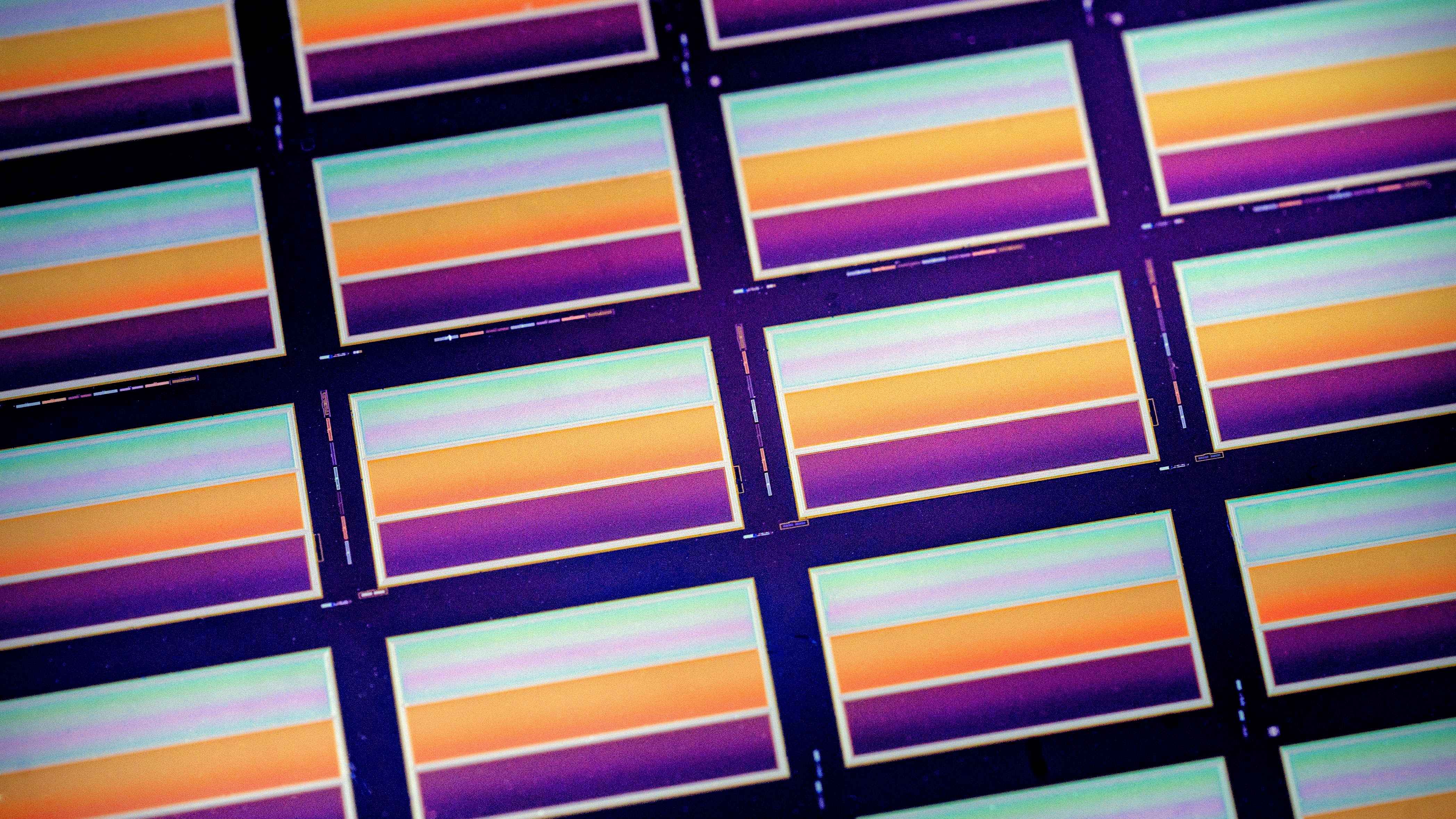
Next-generation sensor for multi- and hyperspectral imaging from space sets new standard in light sensitivity and spectral range
Read more

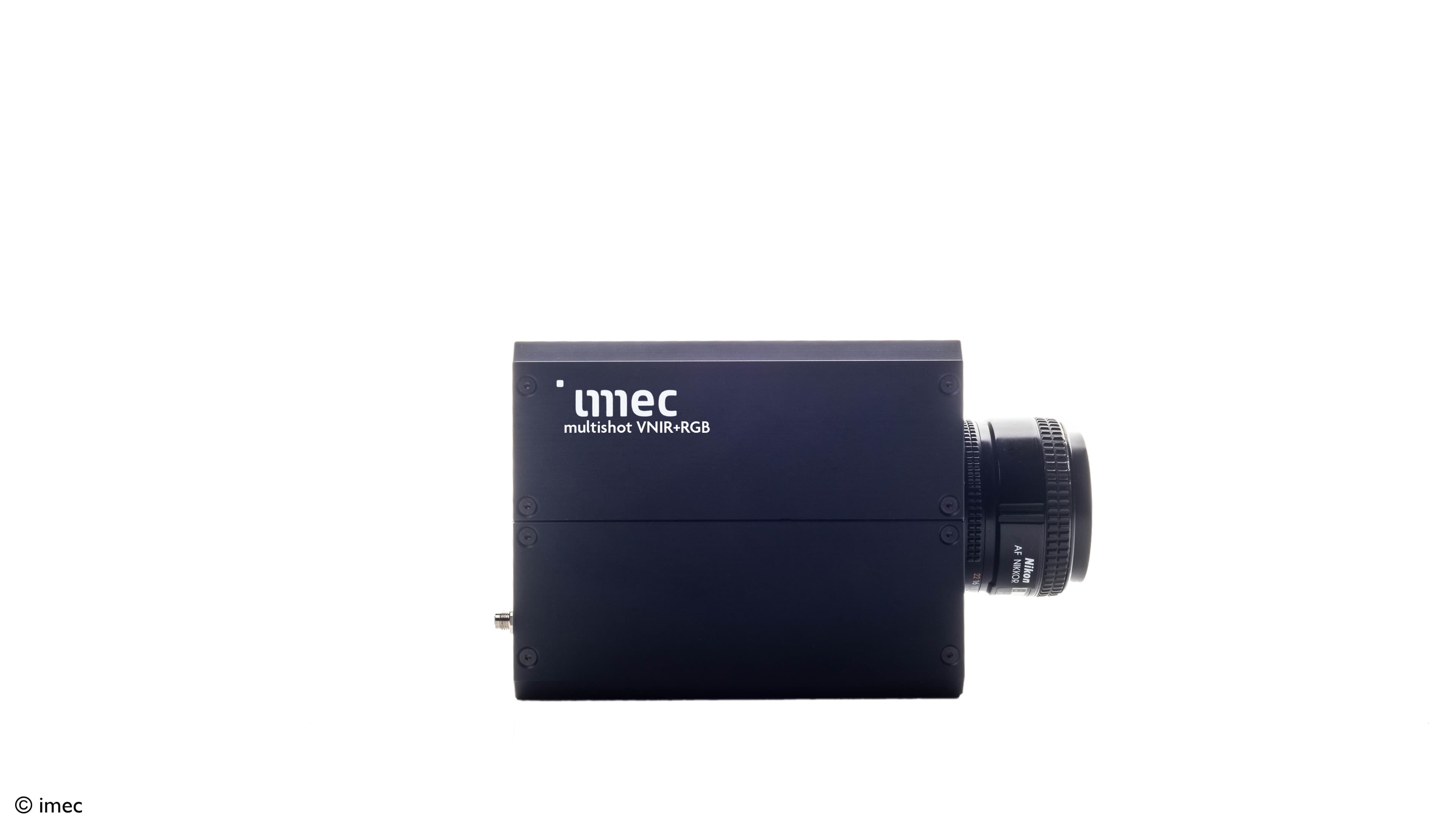
Imec demonstrates combined VIS & NIR spectral camera system, complemented with hi-res RGB imaging, for data acquisition at video rate
Read more