
Prototyping and low-volume manufacturing of silicon photonic ICs
Share your masking and processing costs with other designers to manufacture silicon photonic ICs on imec’s platform.
From telecom and datacom to sensing: many applications stand to benefit from the use of integrated circuits that use silicon photonics to combine passive and active components on a single chip.
Imec’s SOI-based integrated silicon photonics platform (iSiPP) offers you the tools to develop such a photonic integrated circuit (PIC). Through a multi-project wafer (MPW) or shared run, you can affordably manufacture small batches of these PICs by sharing costs with other designers.
Affordable prototyping and low-volume manufacturing through MPW or shared runs
For easy access to low volumes of silicon photonic ICs, IC-Link offers its MPW-service, which allows you to share masking and processing costs with other designers.
Currently, IC-Link offers the following technologies for MPW customers:
- iSiPP50G: 200mm (8”) platform co-integrates a wide variety of passive and active components to support a wide range of optical transceiver architectures at data rates 50Gb/s.
- imec Si-photonics passives+ 200mm (8”) platform a subset of iSiPP50G technology, that combines passive components with metal based heater for thermal tuning.
Our MPW services are provided through the Europractice platform, where imec is one of the partners.
Want even more flexibility? The iSiPP200 platform allows dedicated runs that give you ample options for customization.
Technical details
Si Photonics iSiPP50G
The iSiPP50G platform co-integrates various passive and active components. It supports a range of optical transceiver architectures, at data rates of 25 or 50 Gb/s. You have access to integrated components such as:
- low-loss waveguides
- efficient vertical grating or broadband edge couplers
- SiN waveguides and SiN-based edge couplers
- high-speed silicon electro-optic modulators
- high-speed silicon-germanium electro-absorption modulators
- high-speed germanium waveguide photodetectors.
- option for exposed waveguides (removing oxide from the top of the waveguides so exposing them to ambient).
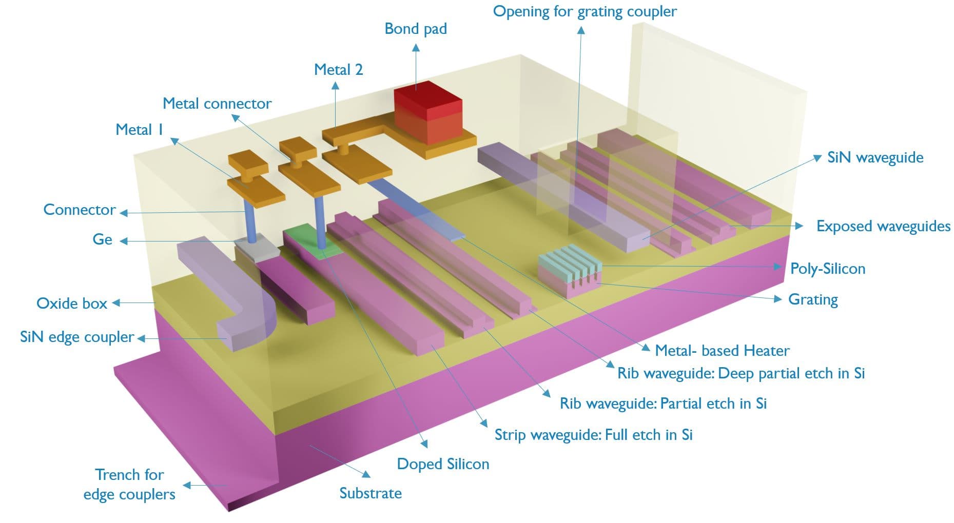
The iSiPP50G platform offers excellent performance and design flexibility, and unrivalled critical dimension and thickness control. It’s a mature process technology (130nm) with a proven device library.
Si Photonics Passives+
Si-Photonics Passives+ technology is a subset of iSiPP50G technology.
Its main features are:
- The device layer of silicon-on-insulator wafers is etched at three different depths. This allows the combination of different photonic functions.
- A patterned poly-silicon layer optimizes the performance of grating couplers for out-of-plane coupling to fibers.
- A deep etched trench at an edge of the ICs, combined with edge-coupler elements, ensures optical access, with a wider optical bandwidth.
- A layer for metal-based heaters permits thermal tuning of the optical functions.
- Electrical access to the metal heaters is created through two supplementary levels of metal interconnects.
- Option for exposed waveguides (removing oxide from the top of the waveguides so exposing them to ambient).
- The imec Si-Photonics Multi Project Wafer service (MPW) serves data- and telecom applications. Although you can also come to us with designs for alternative purposes, such as sensing.
Schedule 2026

Find the complete overview in this Detailed submission schedule file
Prices
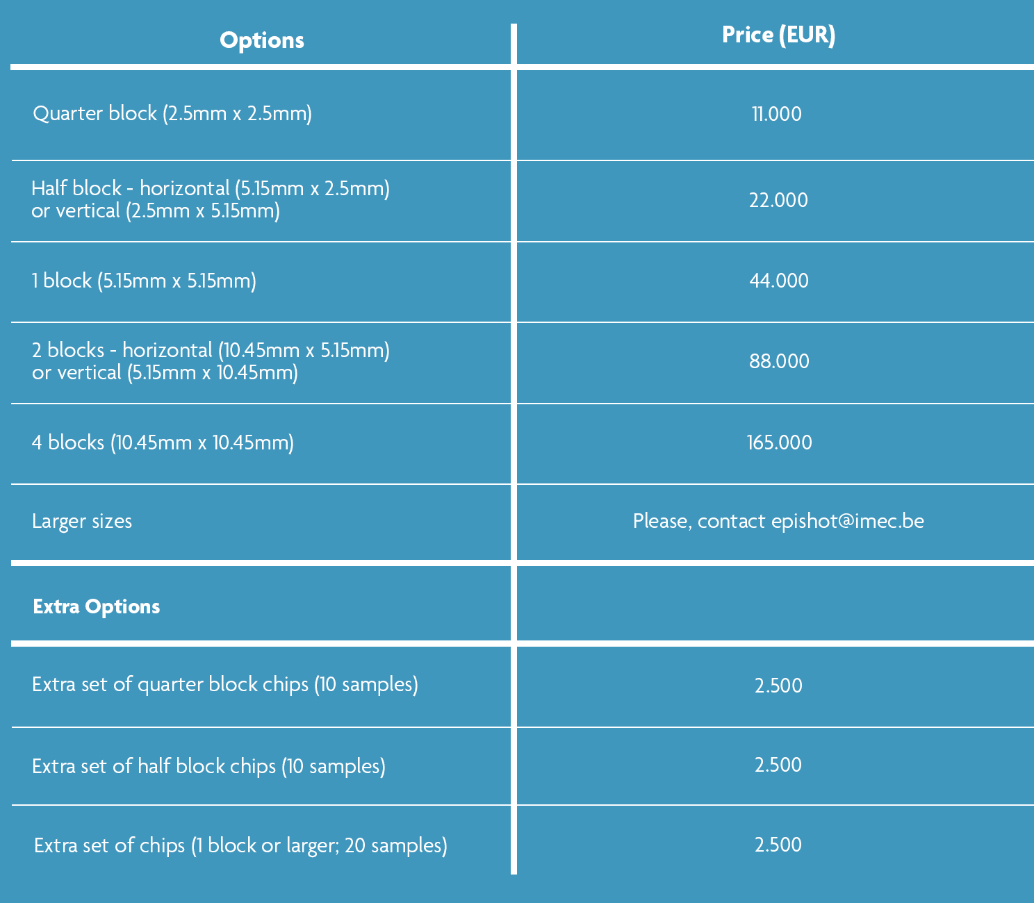
Si Photonics iSiPP50G
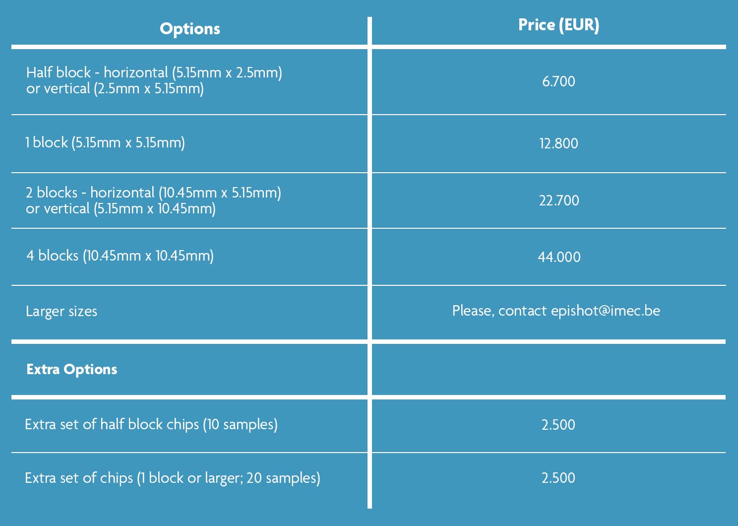
Si Photonics Passives +
Read more

IC-Link selected as a European Design Enablement Team (DET) under EuroCDP
Start-ups and SMEs can now get funded access via the European Commission and member states to chip development.
Read more


IC-Link now also offers silicon nitride (SiN) manufacturing services through imec’s mature platform
Opening a path to commercial production of imec’s low-loss SiN technology will accelerate innovation in datacom and emerging photonics applications such as (bio)sensing and AR/VR.
Read more