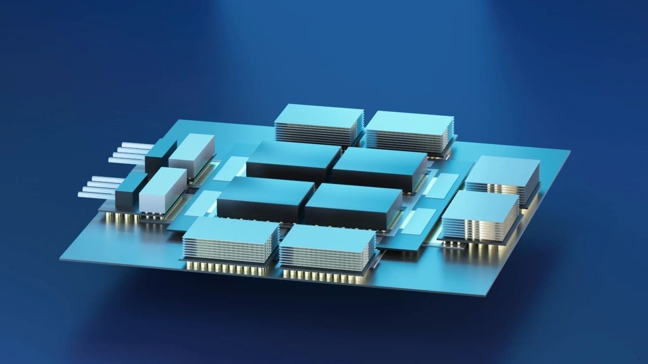
Tackling network-on-chip (NoC) scaling challenges with a system-technology co-optimization approach
Co-integration of NoC routing channels alongside the backside power delivery network: a scalable and cost-effective approach

In short
The routing of the network-on-chip (NoC) scales slower than high-density logic in conventional 2D multi-core systems due to scaling limitations in the metal interconnects.
The article discusses two approaches to scaling NoC: using a dedicated routing die, and integrating NoC channels on the backside.
Backside NoC integration emerges as the more cost-effective solution, leveraging existing backside power delivery networks for improved scalability.
A System Technology Co-Optimization (STCO) approach ensures the effective integration of power delivery, signal routing, and logic elements, addressing challenges like resistance, signal integrity, and manufacturing cost.
As cloud computing demands continue to grow, optimizing multi-core processors for performance, cost, and scalability is crucial. Network-on-Chip (NoC) scaling has become a bottleneck due to conflicting interconnect requirements between the dense logic and the chip communication infrastructure (the physical limits of metal interconnects).
This article examines two approaches to NoC scaling, presented in imec’s latest IEDM paper: a dedicated NoC routing die, and backside NoC signal integration. While both strategies can reduce manufacturing costs at very high bandwidths, backside integration stands out as the more scalable and cost-efficient option by co-integrating signal routes alongside the existing backside power delivery network (BSPDN).
To address the challenges of co-integrating NoC channels with the BSPDN, the researchers applied a System Technology Co-Optimization (STCO) approach. By optimizing the relationship between the BSPDN, logic layers, and NoC routing, the STCO methodology ensures that power, signal integrity, and design complexity are balanced effectively. This coordinated design framework addresses issues like IR drop, latency, and manufacturing costs, making backside integration of signal channels a promising solution for high-performance systems such as cloud server CPUs.
Read the full article, previously published in Semiconductor Digest here.
Authors

Moritz Brunion
Moritz Brunion received the M.Sc. degree in electrical and computer engineering from the University of Bremen, Germany, in 2022. He is currently a researcher at imec, Leuven, Belgium, and his research focuses on design-technology co-optimization for fine-grained 3D systems.

James Myers
James Myers holds a MEng degree in Electrical and Electronic Engineering from Imperial College in London. He spent 15 years at Arm, leading research from low power circuits and systems, through printed electronics, to DTCO activities. He joined imec in 2022 to lead the System Technology Co-optimization program, with the aim of building upon established DTCO practices to overcome the numerous scaling challenges foreseen for future systems. James holds 60 US patents, has taped out 20 SoCs, has presented at ISSCC and VLSI Symposium, and has published in IEDM and Nature.
Discover more

Sony and imec unveil high-density backside connectivity module enabling next-generation 3D chip integration
Read more

ASML, TSMC and imec bring industry-ready 2D-material transistors closer with breakthrough 300mm integration
Read more