How NanoIC's pathfinding PDKs are bridging the gap between academia and industry in the race beyond 2nm semiconductor innovation
The semiconductor industry is undergoing a rapid transformation. Artificial intelligence (AI) applications, such as agentic and physical AI, push compute demands to unprecedented heights, forcing a fundamental rethink of system architectures.
However, as we move to advanced semiconductor technology nodes, academic research has gradually drifted away from industrial practice, limiting academic researchers in driving innovation.
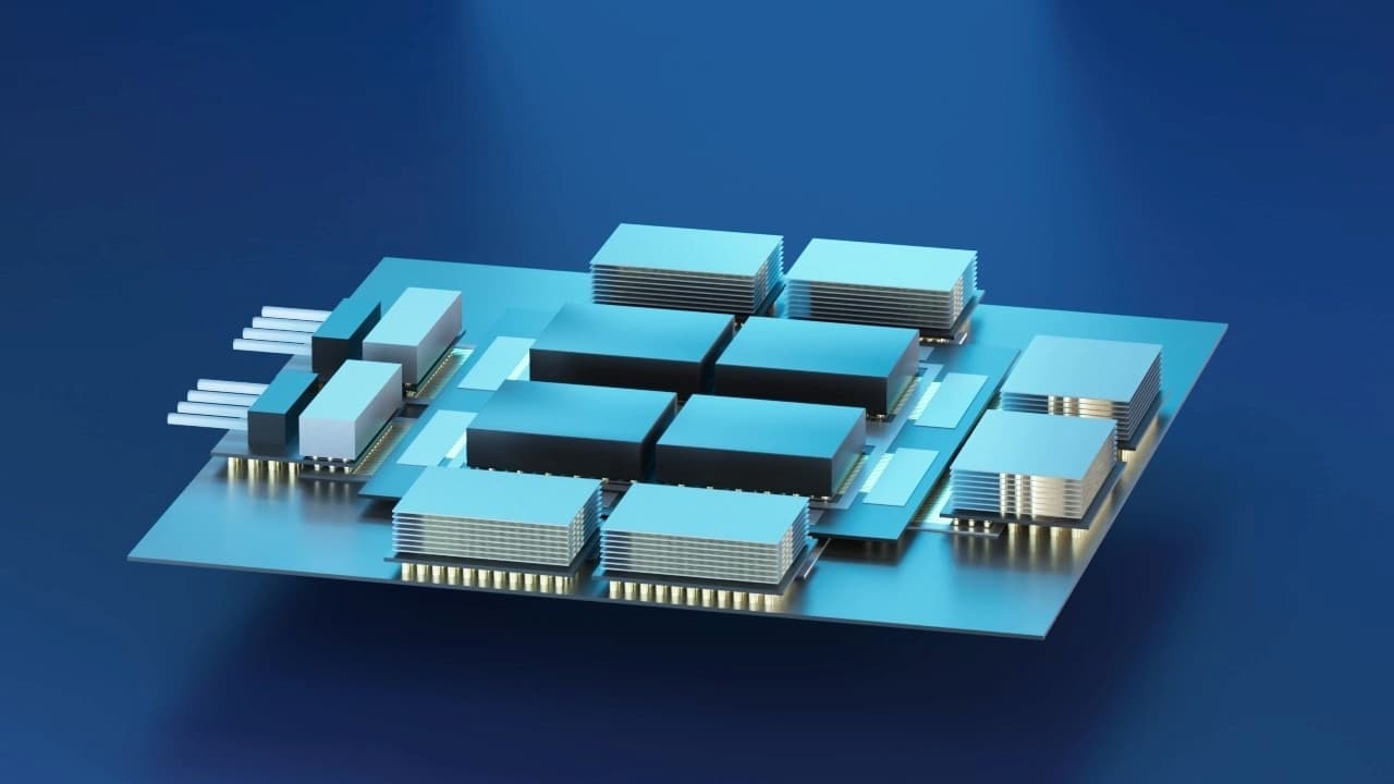
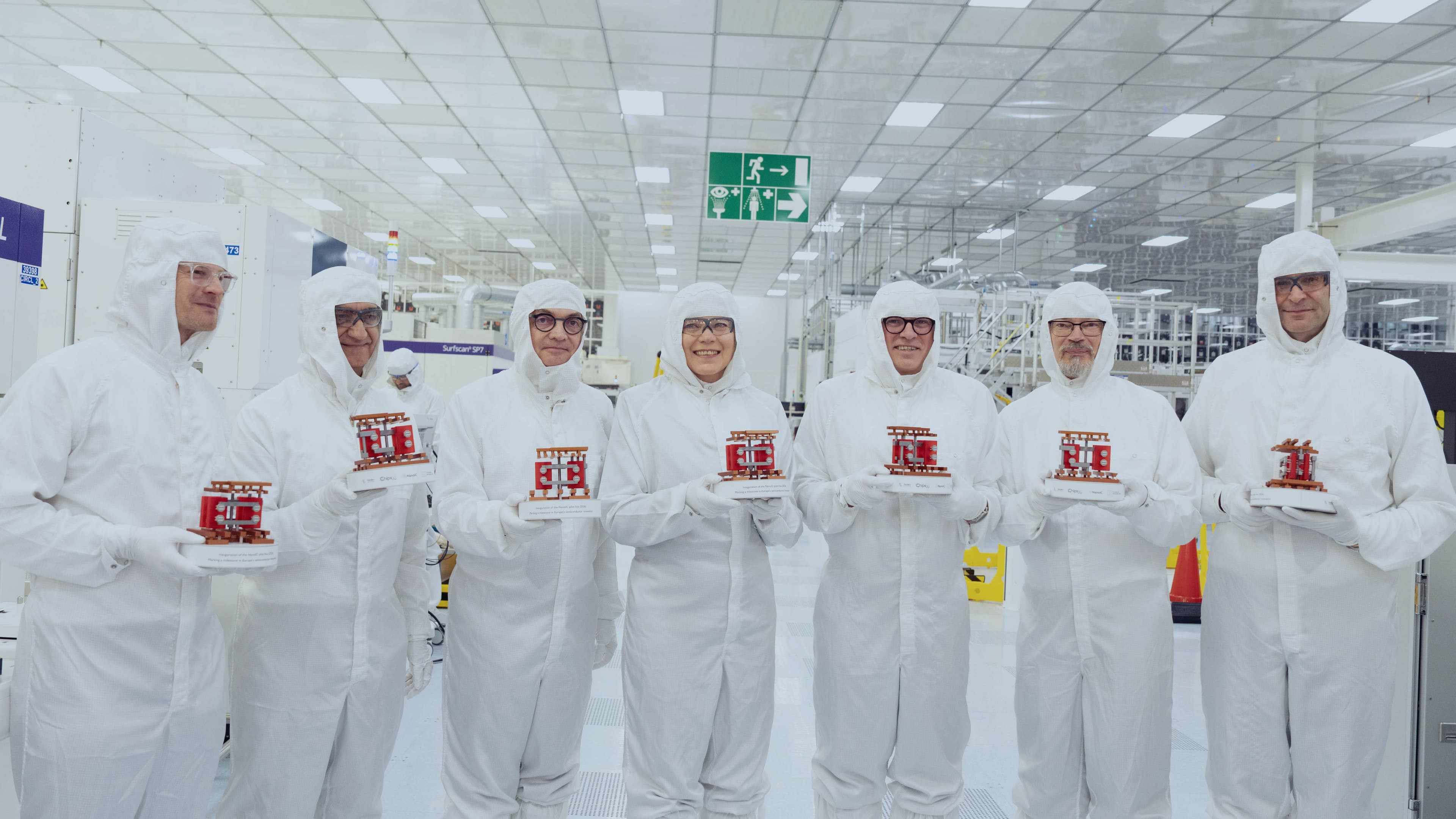
Europe’s NanoIC pilot line, a pioneering European initiative, hosted by imec, aims to bridge this gap with its introduction of pathfinding process design kits (P-PDKs), early-access design kits, enabling researchers to simulate and optimize future chip architectures.
“Historically, universities could conduct meaningful and relevant research at higher levels of abstraction, without detailed access to the underlying technology,” explains Professor Mehdi Tahoori from the Karlsruhe Institute of Technology (KIT). “But with the shift to advanced semiconductor technology nodes, where DTCO (Design-Technology Co-Optimization) and STCO (System-Technology Co-Optimization) are essential, conducting impactful research in computing architectures without direct access to technology has become nearly impossible. As a result, academic research has gradually drifted away from the realities of industrial practice. That’s why the NanoIC pilot line is so important: by providing access to pathfinding PDKs, it bridges the gap between academia and industry.”
Interested in finding out how pathfinding PDKs enable early design exploration? The full article is available on the NanoIC website.
Authors

Anita Farokhnejad
Anita Farokhnejad earned her PhD from Universitat Rovira i Virgili (Spain), specializing in FEOL and device modelling. She joined imec in 2021 as an R&D Engineer, focusing on BEOL optimization and future roadmap development. Collaborating closely with integration and physical design teams, she develops models for PnR data analysis and BEOL optimization. Her recent work on the enhanced Ring Oscillator (eRO) model aids in the early assessment of new materials and BEOL boosters. In August 2023, she advanced to team lead for PDK Enablement, translating advanced semiconductor nodes into Pathfinding-PDKs. Anita is also dedicated to education, conducting courses that make sophisticated technological concepts accessible to both industry veterans and aspiring engineers. Currently, she serves as Program Manager of DTCO at imec, where her contributions continue to drive innovation in the semiconductor industry.
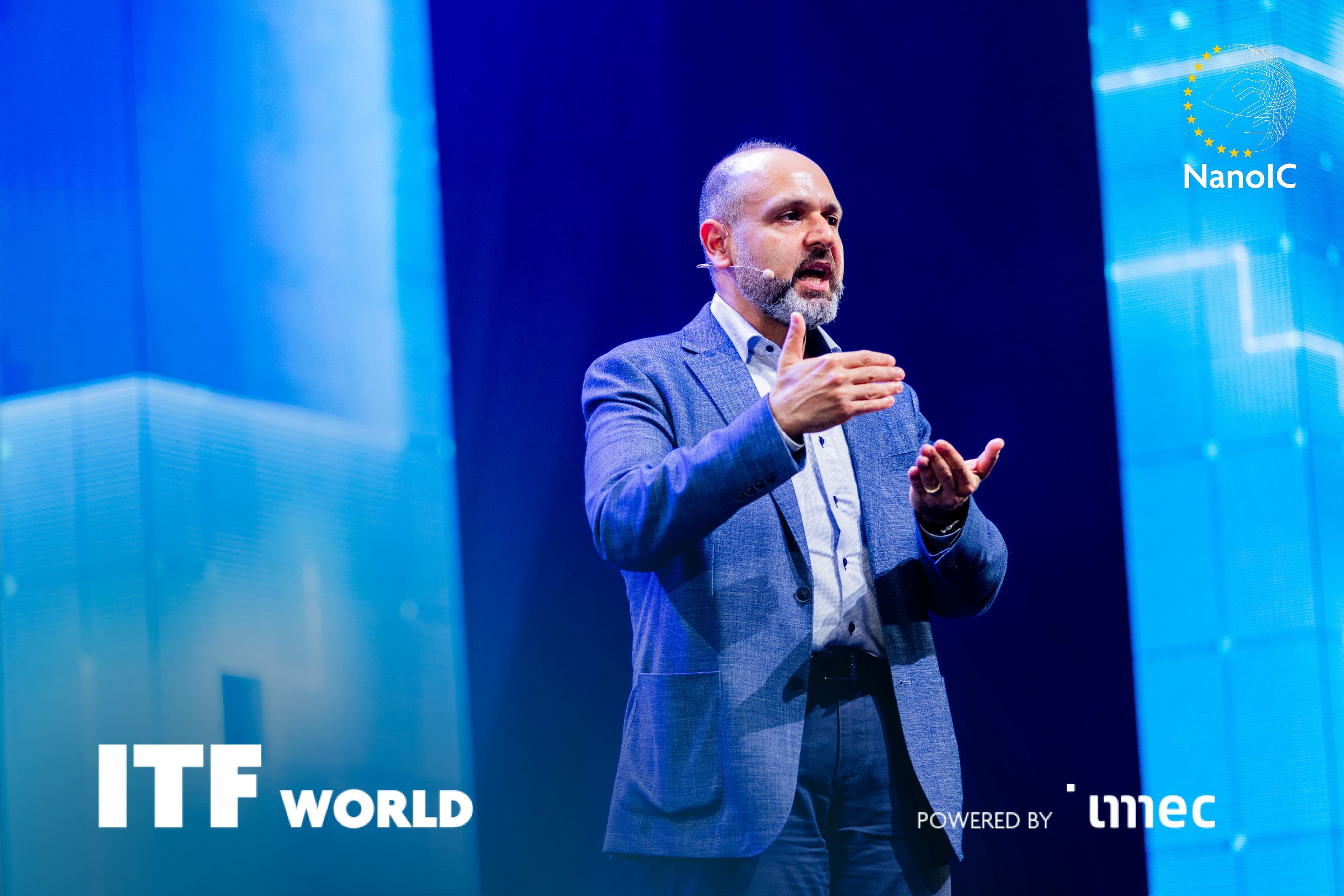
Mehdi Tahoori
Mehdi B. Tahoori is Professor and Chair of Dependable Nano-Computing at the Karlsruhe Institute of Technology (KIT), Germany, and guest professor at imec, focusing on CMOS 2.0 and future chip technologies. He previously worked at Xilinx (USA), Fujitsu Labs (USA), and served as a junior professor at Boston Northeastern University (USA) and as a visiting professor at the University of Tokyo (Japan). He earned his B.S. from Sharif University (Iran) and M.S./Ph.D. from Stanford (USA). Prof. Tahoori is Deputy Editor-in-Chief of IEEE Design and Test Magazine, is a former Editor-in-Chief of Elsevier Microelectronic Reliability and has chaired major IEEE symposia. His honors include multiple best paper nominations and conference awards, the US National Science Foundation Early Faculty Development (CAREER) Award (2008), an ERC Advanced Grant (2022), and an IEEE fellowship.