A non-destructive readout mechanism for ferroelectric capacitors
The demonstration of a non-destructive read operation for FeCAPs presents a milestone towards compute-in-memory applications

In short
Ferroelectric capacitors (FeCAPs) are an energy-efficient alternative to resistive types of memories for analog compute-in-memory (CiM) applications.
However, since conventional read operations for FeCAPs are destructive, the read endurance is limited by the write endurance, which is insufficient for CiM.
Imec and the Georgia Institute of Technology have demonstrated a non-destructive read operation for the first time, enabling fully decoupled read and write endurance.
They achieved a non-destructive read endurance of >1011 and a capacitive memory window of 8.7 (at 0V) – the largest values reported for FeCAPs.
The promise of FeCAPs for compute-in-memory
Compute-in-memory (CiM) has become an attractive computing paradigm to address the memory and power walls in traditional designs for deep learning applications. With CiM, part of the computation needed to run deep learning algorithms can be performed in the memory itself, thereby avoiding moving around gigantic amounts of data between the memory and the processing unit.
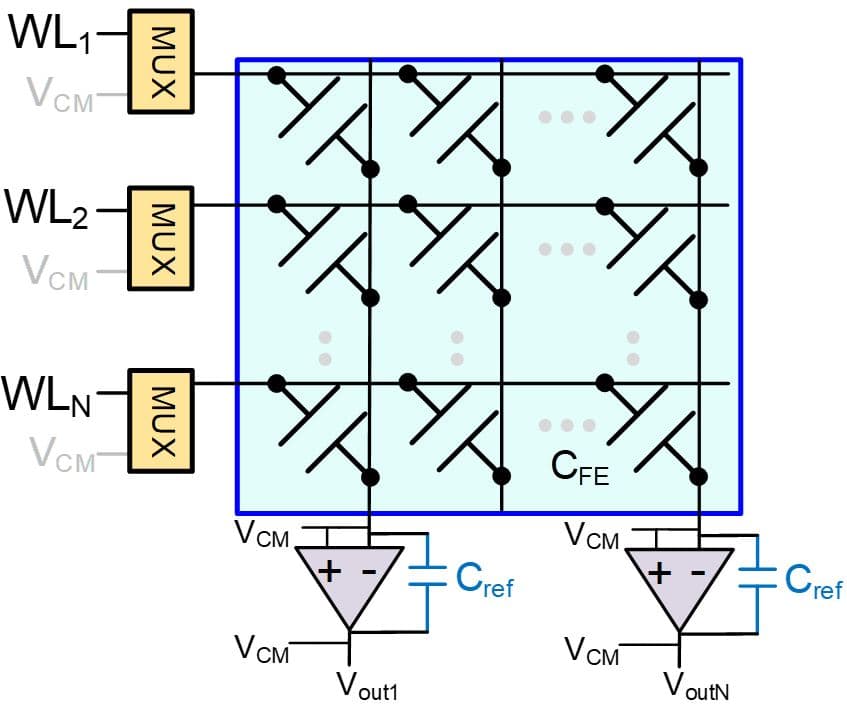
In deep learning algorithms, the dominant operations are matrix-vector multiplications of a weight matrix and an input vector. In these operations, the activation signals from the input vector are multiplied by pre-programmed weights, which are stored in an array of memory elements. The output is the weighted sum of all contributions on the summation line (or bit line).
Different types of non-volatile memory technologies are being investigated for storing the weights. Most popular are resistive types of memories such as resistive RAM (RRAM), phase change memory (PCM), and magnetic RAM (MRAM) – memories that exist in two different resistive states. The memory elements are arranged in crossbar arrays and store the weights as conductance.
A few years ago, researchers at the Georgia Institute of Technology started exploring the possibility of using ferroelectric capacitors(FeCAPs) for storing weights in analog CiM applications. FeCAPs have two major advantages over resistive memories: (1) the circuits have significantly improved power efficiency, and (2) no selector devices are needed since no sneak currents run through the circuits.
The need for a non-destructive read operation
A FeCAP resembles a traditional capacitor but has a ferroelectric material in between two metal layers (the electrodes) instead of a conventional dielectric material. Ferroelectric materials can exist in two electrical polarization states – P+ and P- – which can be reversed through an external electric field. When this field is removed, the ferroelectric material retains its polarization state, giving the FeCAP its non-volatile characteristic.
Today, hafnium-zirconium oxide (HZO) is the ferroelectric material of choice for memory applications because of its scaling potential. However, the conventional scheme to read the polarization state of HZO-based FeCAPs is destructive: it relies on the polarization switching of the ferroelectric material and thus necessitates re-programming the polarization state after each read operation. Consequently, the maximum number of data read operations (i.e., the read endurance) is linked to the maximum number of data write operations (the write endurance). As such, the read endurance cannot be independently optimized. This is a problem for CiM applications, which require virtually unlimited read endurance, while a much lower write endurance is usually sufficient.
FeCAPs with >1011 non-destructive read endurance and ~8.7 capacitive memory window (at 0V)
At the 2023 IEDM conference, imec and the Georgia Institute of Technology presented for the first time a solution that fully de-couples the read and write endurance of FeCAPs. The solution is based on incorporating an asymmetry in the interfaces of the two electrodes. These asymmetrically engineered FeCAP devices could be read out more than 1011times without disturbing the polarization state of the HZO ferroelectric. In addition, a capacitive memory window with a record high value of 8.7 at 0V read voltage was obtained, representing the difference between the relative permittivity of the ferroelectric in P+ and P- state. These results make FeCAP a promising technology for CiM applications.
The mechanism behind the non-destructive read operation
The ability to non-destructively read out FeCAPs with >1011 endurance was partly achieved by looking into the physics behind the readout mechanism. A fundamental understanding of the underlying principles also provides a solid foundation for further improving the results.
Unlike a conventional dielectric material, a ferroelectric material has a non-linear relationship between the applied electric field and the polarization charge, giving the ferroelectric polarization-voltage (P-V) characteristic the form of a hysteresis loop.
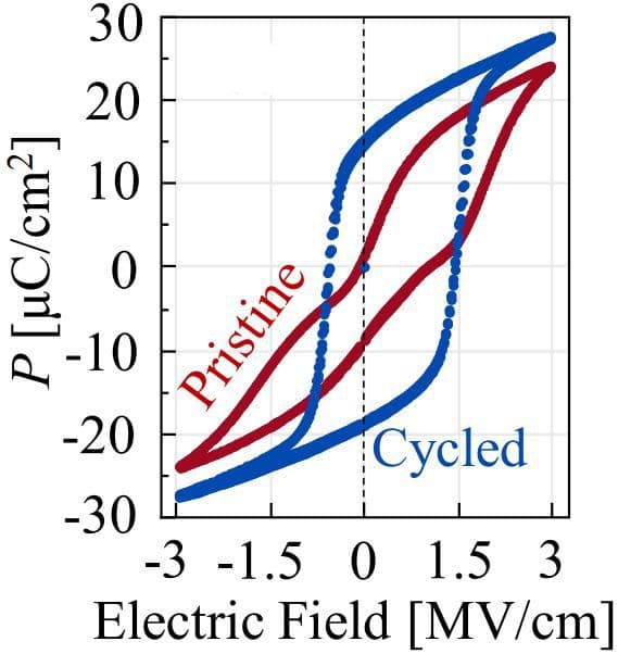
This phenomenon is exploited in conventional reading schemes for FeCAPs. In practice, a voltage pulse is applied to flip the memory cell to its opposite polarization state. When that happens, a displacement charge, equal to the difference between P+ and P- is released and detected. This difference, called the remnant polarization (2PR), represents the memory window. To measure sufficient distinction between P+ and P-, the remnant polarization 2PR should be as high as possible during the entire lifetime of the memory. The main drawback, however, is the need to reprogram the cell after each readout, making the read endurance dependent on the write endurance.
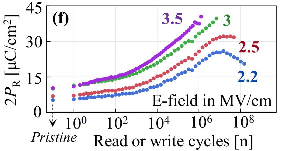
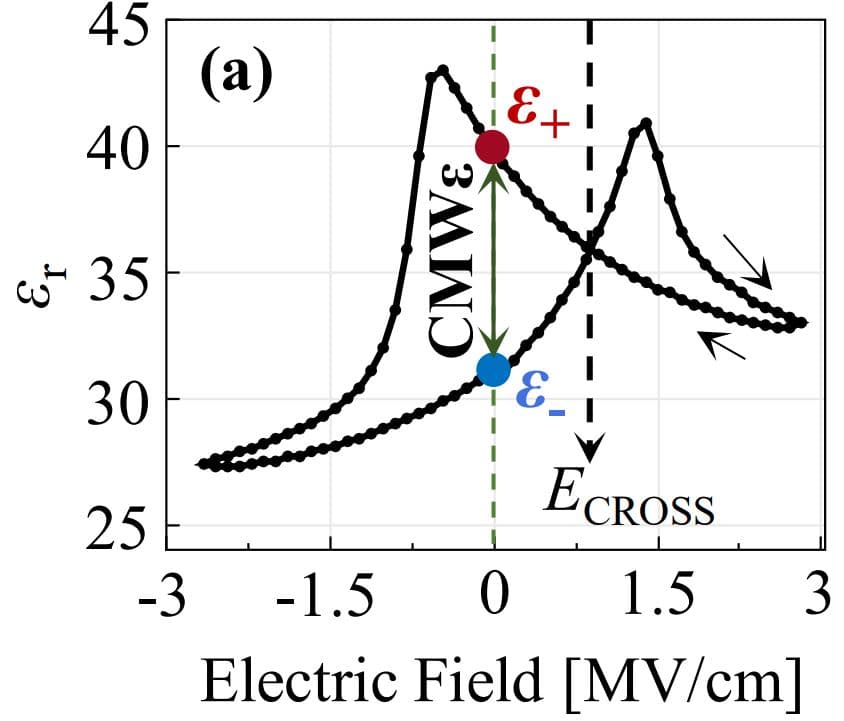
Researchers at the Georgia Institute of Technology and imec take a different approach. They start from a different concept of the memory window. Instead of exploiting the difference between P+ and P-, they use the concept of a capacitive memory window. This capacitive memory window is the difference between the capacitive states of the FeCAP when in either the P+ or P- state. It can be derived from C-V measurements, which plot the non-linear capacitive response (or relative permittivity (εR)) of the ferroelectric material to an applied electric field.
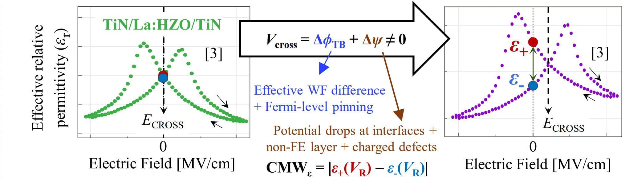
The C-V curve of a ferroelectric capacitor resembles a symmetrical butterfly curve around 0V, as illustrated in the left part of Figure 4. At 0V (or zero electric field), the positive and negative branches of the butterfly curve cross over, resulting in a zero capacitive memory window. But, the research teams found a way to open the memory window at 0V by applying a difference in work function for the two electrodes (see the right part of Figure 4). After interfacial engineering of the electrodes and further optimization of the material stack, a capacitive memory window as high as ~8.7 could be obtained at 0V.
Applying quasi-static C-V measurements to read out FeCAPs is, however, not a circuit-friendly read operation. As a final step, the researchers showed that the same information can be retrieved by applying a pulse-based reading scheme and reading out charges, which is more commonly used in memory operations. With this reading scheme, they achieved non-destructive read endurance of >1011 cycles at 0V DC bias without having to apply the electric field at which the polarization switches (i.e., the coercive field). This scheme allows a complete decoupling of read endurance from write endurance.
Outlook: improving the performance; expanding the application field to FeRAM; towards 3D ferroelectric memories
Research is ongoing to improve further the read endurance and capacitive memorywindow of FeCAPs for CiM applications. This is approached by further engineering the material stack and work function of the electrodes. The capacitive memory window can also be further enlarged by applying the AC read pulse on top of a non-zero DC bias. In this case, however, care must be taken not to exceed the coercive field.
In addition, researchers at imec are investigating the feasibility of using FeCAPs and the non-destructive readout scheme in DRAM-like FeRAM memory applications (embedded and standalone). There are, however, some striking differences between classical active memory and CiM-type operations. For example, for active memory applications, on top of a high read endurance, a much higher write endurance is required than in CiM operations. In addition, in CiM, all memory cells’ (small signal) contributions on the same bit line are accumulated before measuring the outcome. However, in classical memory applications, the state of each individual cell must be reliably measured. This poses more stringent requirements on the magnitude of the readout signal of each individual FeCAP, requiring larger memory windows. The team is exploring the specifications for FeRAM applications and how to achieve them.
For both applications, the expected trend is to go to the 3rd dimension to increase the memory density further. FeCAPs will, therefore, move from planar to 3D capacitorstructures, enabled by the atomic layer deposition process available for HZO-based capacitors. In the longer term, FeCAP-based memories could be integrated on top of peripheral logic circuits. Two features of the presented process technology make this possible. First, as explained before, no selector devices (usually a transistor) are required due to the absence of sneak currents. This enables embedding the ferroelectric memories in the back-end-of-line (BEOL) of the logic circuits. Second, the thermal budget needed for fabricating the HZO-based FeCAPs – such as the low-temperature ALD process – is below 400°C, making the technology fully BEOL compatible.
Conclusion
For the first time, researchers from imec and the Georgia Institute of Technology have demonstrated the feasibility of reading out FeCAPs in a non-destructive way, thereby fully decoupling read and write endurance. A non-destructive read endurance >1011 could be demonstrated, while the write endurance was around 107. The readout mechanism is based on the concept of a capacitive memory window, for which a record-high value of 8.7 could be demonstrated. These results make FeCAPs promising candidates for CiM applications. In addition, the innovations lay the groundwork to explore the FeCAP’s potential for embedded and standalone FeRAM memory applications.
This article was originally published in EDN.
Want to know more?
More details can be found in the article ‘Pulse-based capacitive memory window with high non-destructive read endurance in fully BEOL compatible ferroelectric capacitors,’ S. Mukherjee et al., IEDM 2023.
Interested in receiving this article? Fill in our contact form.
Authors

Jan Van Houdt
Jan Van Houdt received a Ph.D. from the KU Leuven. During his PhD work, he invented the HIMOS™ Flash memory, which he transferred to several industrial production lines. In 1999, he became responsible for Flash memory at imec and as such was the driving force behind the expansion of imec’s Industrial Affiliation Program on Memory Technology. Jan has published more than 300 papers in international journals and accumulated more than 250 conference contributions (incl. ~50 invitations and 5 best paper awards). He has filed about 80 patents and served on the program and organizing committees of 10 major semiconductor conferences. In 2014, he received the title of IEEE Fellow for his contributions to Flash memory devices. In the same year, he started the Ferroelectrics program at imec and became a guest professor at the KU Leuven teaching on CMOS and memory technology. Today, he is Scientific Director at imec, active both in the memory as well as in the logic scaling programs.