How to pick the technology node for your ASIC?
Navigating the complexities of technology node selection is essential for ASIC success. Here, we present some preliminary insights to help you get started on this journey.

In short
Understand what is meant by technology node.
Learn how to pick the right node for your application.
Explore some general guidelines on nodes for applications.
Have you chosen to pursue an application-specific integrated circuits (ASIC)? Good call, because ASICs offer significant competitive advantages. Now, one of your first tasks is to select the appropriate technology node.
What do these technology nodes entail? Why do they matter so much? And how do you choose one that fits your application? Get to know the considerations in this article and don’t hesitate to get in touch for tailored advice.
Smaller, faster, more energy efficient
The technology node, or process node, refers to a specific foundry process that defines the chip’s characteristics.
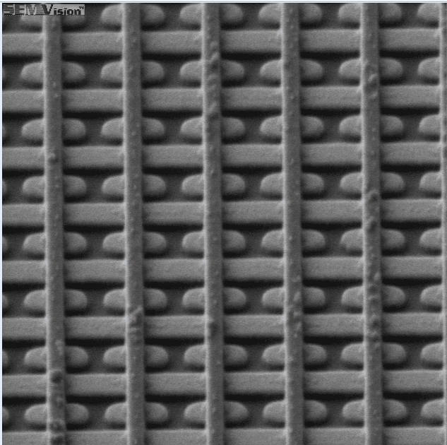
One of those characteristics is size. Smaller chip features mean you can fit more transistors on a chip. That results in higher speeds and lower energy consumption. This is what’s known as traditional scaling at the pace of Moore’s law.
The importance of this dimensional scaling is reflected in the fact that technology nodes are usually expressed in nanometers, such as TSMC's 28nm process. 28nm is the actual gate length of the MOS transistor used in this technology. However, going to advanced-node technologies the number no longer directly corresponds to a physical feature of the transistor. For instance, TSMC's N3 technology uses 3D transistors where gate length is no longer relevant.
Another characteristic is the transistor architecture. This is strongly related to size, because as we continue to shrink transistor sizes we’re encountering physical limitations that necessitate rethinking transistor structures.
The older CMOS technology nodes used the traditional ‘planar’ transistors. Starting around the 16nm node, foundries moved towards FinFET architectures. And the newest chips are built using gate-all-around (GAA) technology.
To conclude, every new technology node results in chips that are more compact, faster, more energy efficient – and thus more sustainable in operation – than those of the previous generation.
Fit for purpose
So why not choose the most advanced technology node for your ASIC? Because those benefits come with a cost. The smaller the node, the more complex and more expensive the manufacturing process. That means you need to carefully consider which advantages do or do not warrant the extra costs.
At the design level, a more advanced process comes with specific possibilities and/or challenges in terms of new design rules, and (non-) existing IP. It also affects the availability of so-called more-than-Moore processing options, such as non-volatile memory, high-voltage functions and even non-electronic components such as microfluidic channels.
Last but not least, the technology node also dictates which packaging techniques are available. And those are becoming increasingly important for speed and power gains.
Choosing a technology node is therefore a question of assessing the balance of what value the node adds vs. the costs it involves. That judgment can only be made when taking your application into account.
Aligning technology nodes with application domains
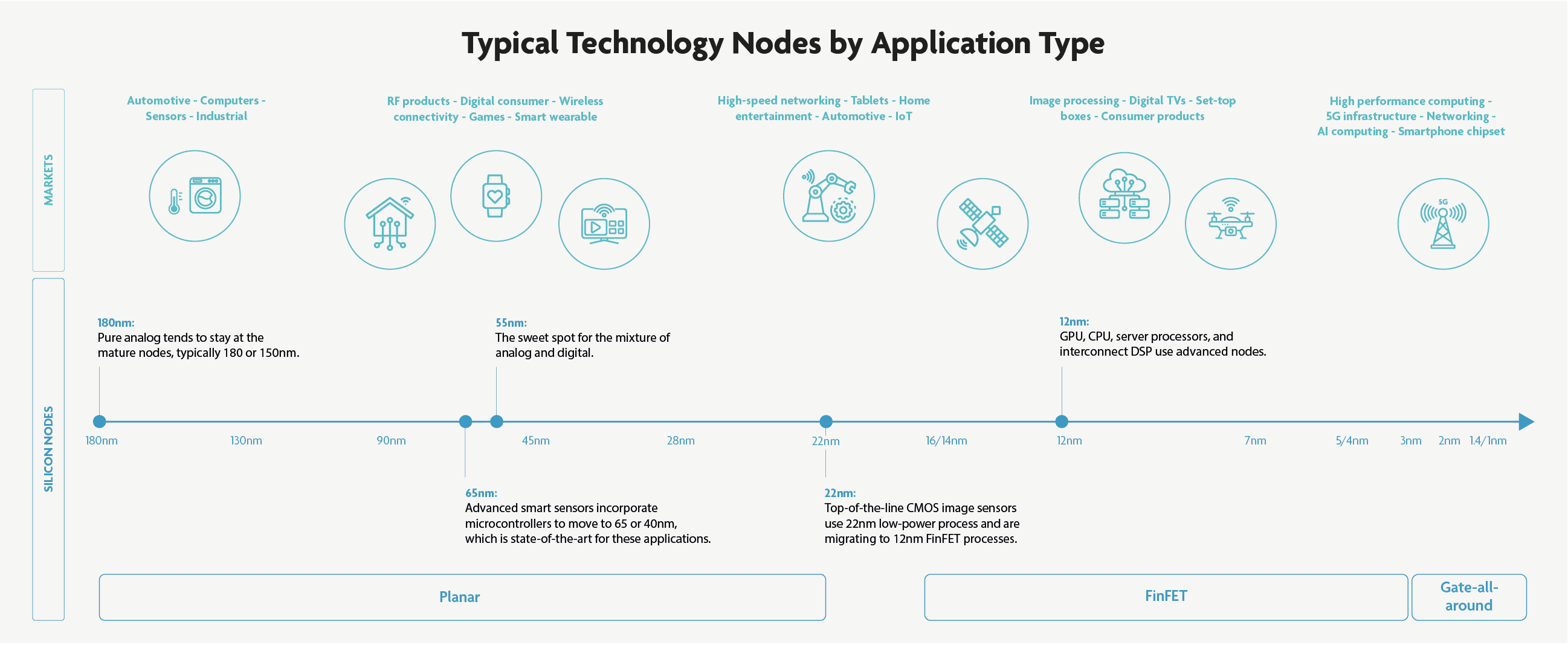
Precise technology node selection is a job for specialists that look at dozens of variables. However, here are some general guidelines. They’re not strict rules and might change in the future. But they give you some idea of how the requirements of broad application domains match with certain process nodes.
Smart home devices and sensors, as well as relatively simple wearables, combine a compact form factor with a processing power of 1 tera operations per second (TOPS) and limited AI performance. They’re best served with a microprocessor or neural processing unit (NPU) paired with an ASIC in one of the mature nodes (i.e. TSMC 22nm or larger). These provide sufficient processing power coupled with compactness and energy efficiency.
More advanced Edge AI needing 10 TOPS, such as fitness trackers and virtual home assistants, benefit from ASICs built on 28nm-7nm technology nodes. This allows to prioritize performance within strict form factors and power constraints.
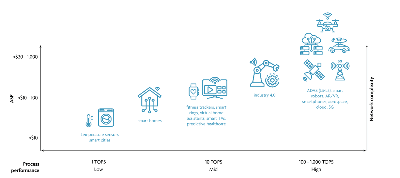
Finally, there are those high-performance applications in automotive, data-/telecom and high-performance computing that require thousands of TOPS. For these, you need to leverage ASICs and GPUs built on the 5nm technology node and below. To reduce even more the cost of the device, chiplet architectures – the heterogeneous integration of modular chips – can come into play.
From technology selection to execution
Do you have a rough idea of which process node fits your application? Then the next step is to define the precise technological requirements. And, finally, to find the resources you need to fulfill them: from design capabilities (including packaging design) to IP, foundry services, packaging, testing and qualification.
Our team is ready to guide you through that process. We combine in-house technical and application-specific expertise with a strong network among all levels of the semiconductor value chain and ecosystem. Making sure your ASIC is delivered according to expectations, within budget, and on time. Ready to empower a product that transforms your market.
Click the button below to get in touch.
Discover more