20-year semiconductor roadmap: tearing down the walls
Deep tech, enabled by semiconductor technology, will provide disruptive innovations that are essential for tackling humanity's monumental challenges. The transformation of industries such as the medical industry will require the handling and analysis of exponentially growing amounts of data, demanding enormous computing power.
To enable this sustainably, we need an even more aggressive semiconductor roadmap than what we have achieved over the last decades. In this article, Luc Van den hove, President and CEO of imec proposes a roadmap that will continue to enable more performant semiconductor technologies.

This article was originally written and published by Pete Singer, Editor-in-Chief at Semiconductor Digest.
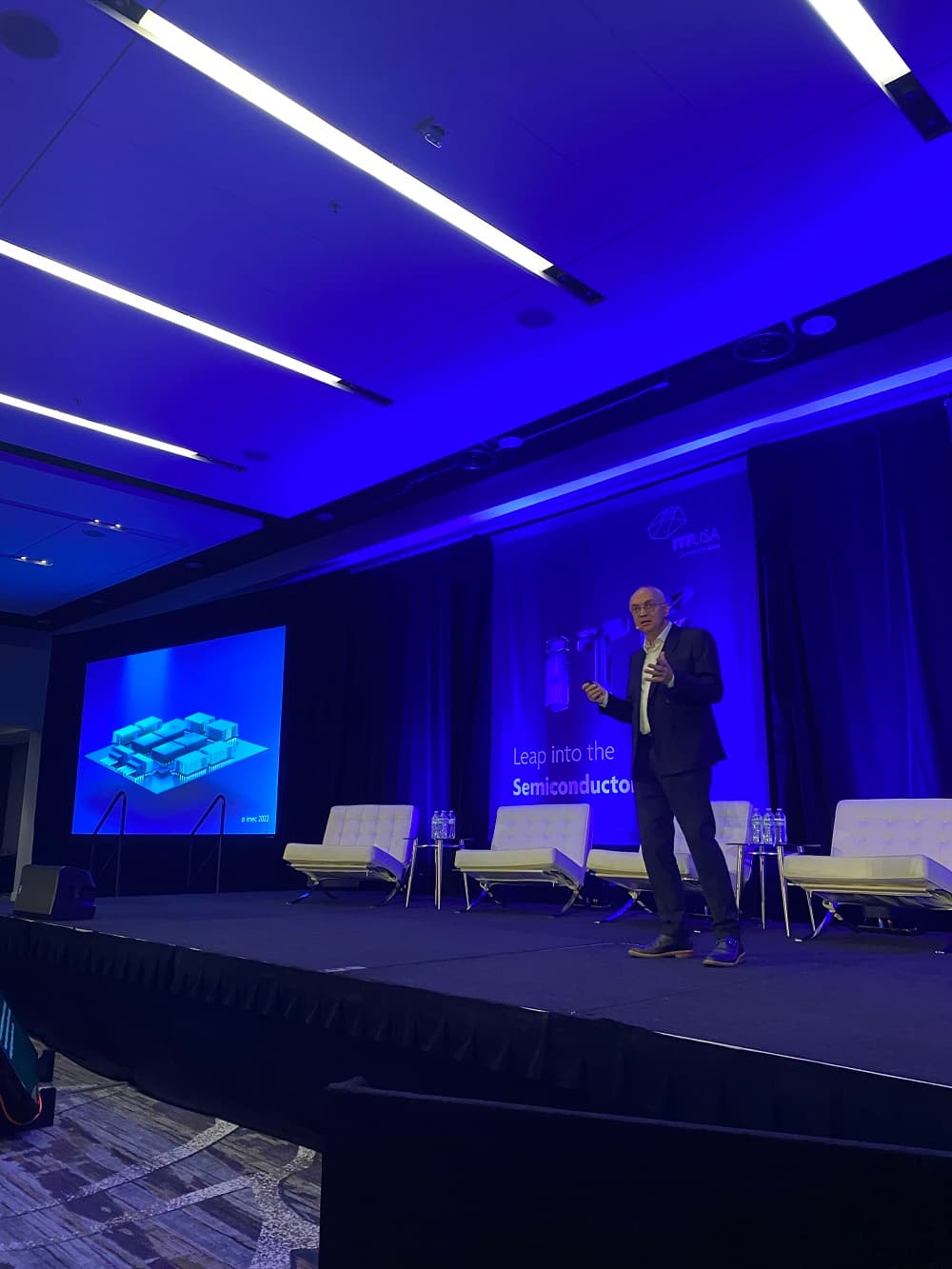
On Monday 11 July 2022, in advance of SEMICON West, imec hosted its annual International Technology Forum (ITF USA). Luc Van den hove, president and CEO of imec, presented his view of a 20 year technology roadmap which he said is even more aggressive than what the industry has achieved over the last decades.
“We will leverage our core semiconductor expertise to realize deep-tech innovations by co-innovating at the semiconductor technology, system and application levels. And by leveraging expertise from many domains such as material science, biomedical, pharma, AI, and others,” Van den hove said.
Building flourishing deep-tech ecosystems must become a priority to meet the challenges of the 21st century. That includes those in the medical field, addressing the food shortages, tackling climate change and air pollution, and finding solutions for sustainable mobility. “All of these challenges require us to develop real deep tech technology solutions,” Van den hove said. “They will require massive data handling, and we therefore need to make our technologies more and more performant.”
The semiconductor industry has long relied on traditional Dennard’s-based scaling, which simultaneously provided increased performance and increased density at a reduced power and a reduced cost. “This one-dimensional version of the roadmap may not be sufficient anymore for the future,” said Van den hove. “We will have to tune our devices for specific applications.”
Traditional scaling is hitting multiple walls in terms of power, performance, scaling and cost. “Just the lithography-based shrinking is getting harder,” Van den hove said. “It’s not stopping, but it’s getting harder and harder. The performance improvement that we are used to for single transistors from node to node has been slowing down. This is why we had to go to massive parallelization.”
System performance becomes increasingly dominated by data path limitations between the core processor and the memory. That creates data handling limitations, particularly in AI applications. “This is what we refer to as the memory wall. Memory peak bandwidth cannot keep up with processor peak throughput,” Van den hove said.
Another wall is the power wall “It becomes harder and harder to get all the power into our chip, but also to extract the heat out of each chip. Therefore, we need new cooling techniques,” he said. Cost is also exploding (the cost wall), which needs to be compensated by the complexity increase.
"Traditional scaling clearly is hitting many of these walls. We will have to develop technology solutions actually to tear down those walls in order to enable the continuation of Moore’s Law", Van den hove said.
For this wall tear-down, a multitude of approaches are needed. Those include dimensional shrinking, the development of new switches/transistors, increased use of the third dimension, and a system-level approach to design optimization.
High-NA EUV needed in 3 Years
Imec hosted some of the earliest work on EUV, and Van den hove said the lithography roadmap experienced a 'phenomenal boost' recently with the introduction of EUV into high-volume manufacturing.
“This happened at the five-nanometer node. It was much harder than originally expected. It took much longer, but thanks to the phenomenal dedication and commitment of companies such as ASML and Zeiss, it happened,” he said. “The current version of EUV we believe will be extendable down to the two-nanometer generation or maybe even a node further. But to go beyond that, we will need a next version of EUV.”
This will require bigger lenses and new system platforms to be developed. The optics must adhere to phenomenal specifications, 20-picometer accuracy over for a lens with a diameter of one meter. “If we extrapolate this to the size of the earth, it means that we would have to polish the earth with an accuracy of the thickness of a human hair. This is unbelievable, mind-boggling,” said Van den hove. “We expect that the first machines will be ready next year.”
Introduction of high-NA EUV will also create many challenges on the process side. “In order to address those in a proactive way, we’re setting up, together with ASML, a joint high-NA lab built around the first prototype machine. This will be interfaced to a TEL track and surrounded with the most advanced metrology capabilities. We're doing that because the challenge to introduce high-NA EUV in a timely fashion will be tremendous,” Van den hove said.
“It took us about 10 years to go from the first EUV scanner to insertion into high-volume manufacturing. For high NA, we will have much less time, only three years. In order to derisk that introduction in manufacturing, we are setting up a very intensive program. Here, we develop all the key enabling building blocks, such as the mask technology and the materials using wet or dry UV resist, metrology and optics characterization.”
Device innovations on the semiconductor roadmap
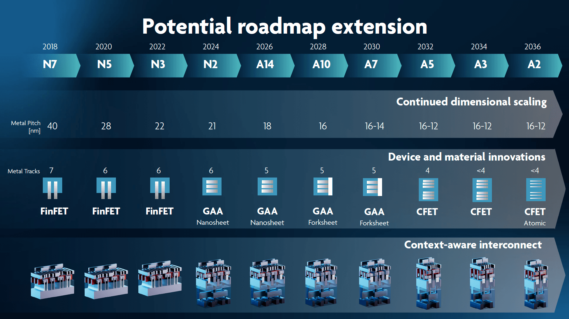
Van den hove described several proposed innovations for disruptive transistor architectures in order to enable further scaling. Those include a gate-all-around device built up of a stack of nanosheets, and a new transistor concept called the forksheet device in which the N and the P channel transistors are moved closer together.
“This forksheet device, we see as an extension of the standard nanosheet concept. We believe it will be introduced around the equivalent of the one-nanometer generation,” Van den hove said. He also described an option where the N- and the P-channel transistors are stacked on top of each other, called a complimentary FET (cFET) device.
“It’s clear that you can realize another very important step in cell size shrinking. That's obviously at the expense of much more complex contacting schemes to contact the source and drain areas. But we believe that we have developed integration schemes that would enable such transistors by optimizing the epi processes and patterning processes. And by leveraging very sophisticated deposition processes to enable the contacting structures,” said Van den hove.
Other innovations include reducing the thickness of the silicon channels to reduce channel length. This could be enabled through the use of new materials, replacing the silicon with 2D materials — atomically flat mono layers — such as tungsten or molybdenum sulfides or selenides. “We’ve recently demonstrated the first versions of devices fabricated using 300 millimeter equipment,” he said.
20-year semiconductor roadmap
Van den hove said a combination of continued dimensional scaling, new transistor architectures, new materials introduction, combined with innovative interconnect architectures (buried power rails) will be the secret to success. “We believe that we can propose a roadmap for the next eight to ten generations — with an introductory pace of two to two-and-a-half year cadence. That would give us a roadmap for the next 20 years.”
This article was originally written and published by Pete Singer, Editor-in-Chief at Semiconductor Digest. See original publication here.
Discover more

Sony and imec unveil high-density backside connectivity module enabling next-generation 3D chip integration
Read more

ASML, TSMC and imec bring industry-ready 2D-material transistors closer with breakthrough 300mm integration
Read more