Stefaan Decoutere
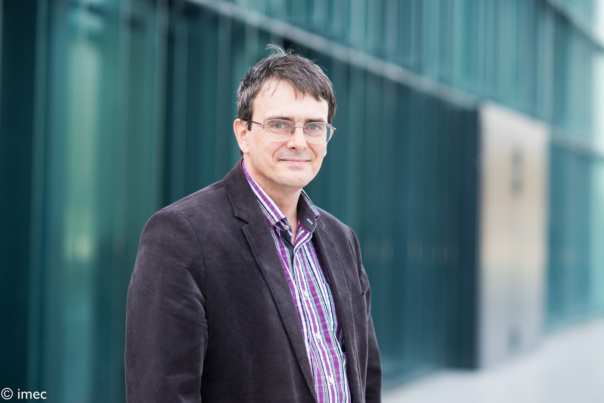
Stefaan Decoutere received the M.Sc. degree in electronic engineering and the Ph.D. degree from the Katholieke Universiteit Leuven, Belgium, in 1986 and 1992 respectively. He is with imec, Leuven, since 1987, where he started in high-voltage BCD technology development. From 1992 till 1997, he was in charge of the development of high-speed BiCMOS and SiGe HBT technologies. In 1998, he became the head of the mixed signal/RF technology group in imec. Since 2010 he manages the GaN power device technology development, and in 2015 he became the director of the GaN technology program.
Authored articles

Unlocking the full potential of GaN technology for next-gen power electronics
Improving GaN device architectures, substrates, and IC design to boost power conversion efficiencies across industries.
Read more
Meet imec fellow Stefaan Decoutere
“Don’t only work out a topic in depth – develop a broad skillset that helps to put your work in a broader context”
Read more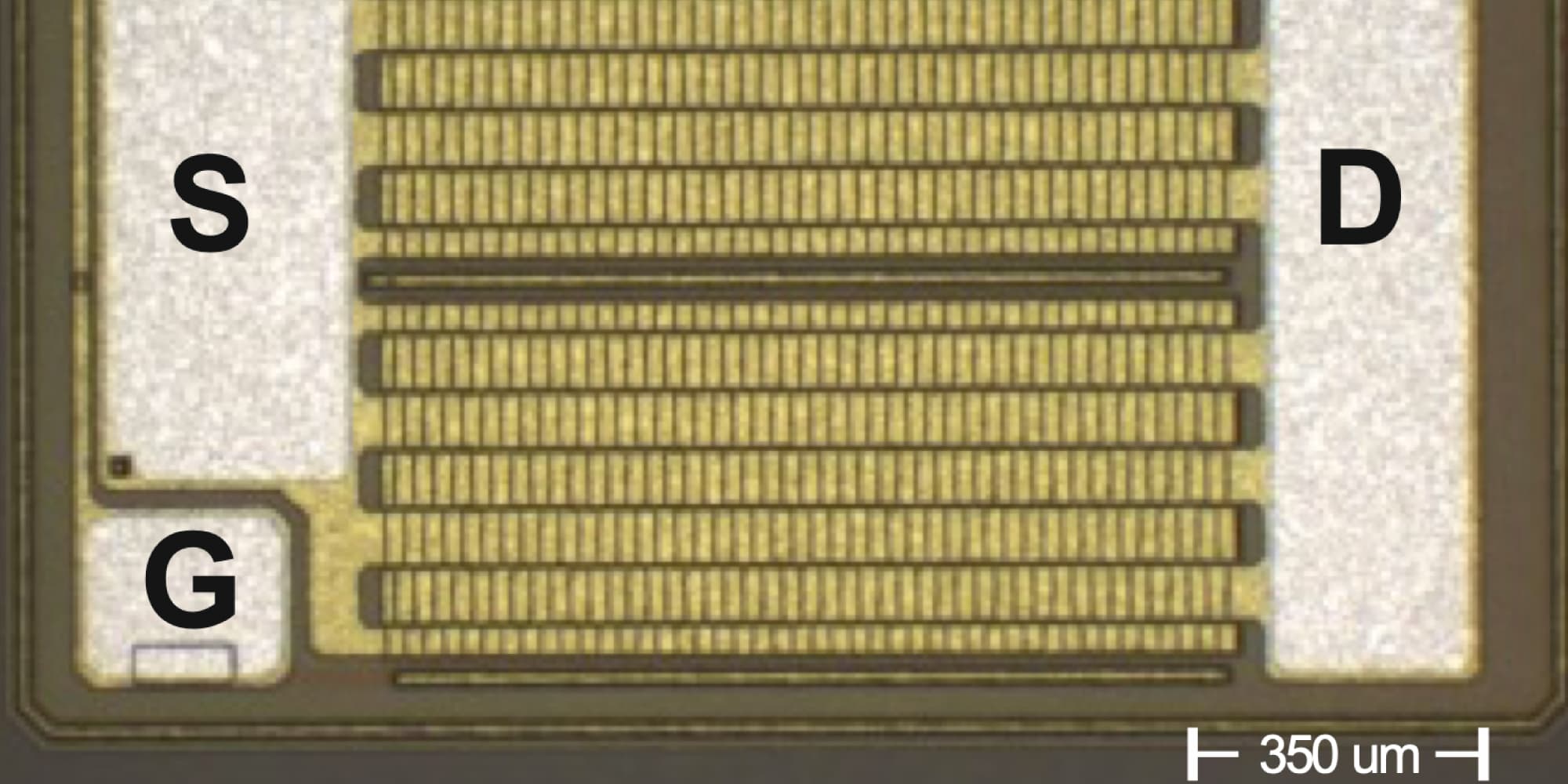
Monolithic integration of GaN components boosts power integrated circuits
The successful cointegration of high-performance Schottky barrier diodes and depletion-mode HEMTs on a 200V GaN-in-SOI power IC
Read more
A new generation of power electronics will make electric cars more efficient and cheap
European ‘HiPERFORM’ to introduce wide-bandgap power electronics in next-generation electric cars.
Read more
Packaging solution for GaN-on-200mm Si power devices
Imec and UTAC have developed a unique process for the wafer thinning and backside metallization of highly stressed GaN-on-200mm Si wafers. This has resulted in a packaged 650V GaN device – smaller than state-of-the-art.
Read more