What’s cooking in imec’s sustainable-semiconductor program?
With more partners joining the Sustainable Semiconductor Technologies and Systems program, it’s time to tune in on the vision and milestones.

In short
Less than a year after its official launch, some of the leading consumer electronics and semiconductor manufacturing players have signed up as partners in imec’s program for Sustainable Semiconductor Technologies and Systems (SSTS).
The program assesses the environmental impact of new technologies, identifies high-impact problems, and defines semiconductor manufacturing solutions with less environmental impact.
In this way, the program gathers the semiconductor value chain to jointly target net-zero emissions for chip manufacturing.
Ecological footprint
Today, IC manufacturing is estimated to account for about 0.1 percent of global emissions. However, forecasts indicate that this percentage could increase to around 1.5 by 2030 if the semiconductor sector remains passive while other sectors stick to the Paris Agreement. With a projected annual growth of eight percent in wafer volume and the accompanying rise in emissions from the complexity increase of each future technology generation, the semiconductor manufacturing industry must step up to avoid seeing an unacceptable rise in its ecological footprint.
There are still significant challenges ahead for the semiconductor industry to meet its sustainability ambitions.
Most of the leading semiconductor players subscribe to the ambition of becoming completely carbon neutral or net-zero between 2030 and 2050. Many companies are already actively managing their carbon footprint and have made substantial progress in lowering their emissions. Yet, with nearly 75 percent of a mobile device’s carbon footprint being due to its fabrication, it’s clear that there are still significant challenges ahead for the semiconductor industry to meet its sustainability ambitions.
More uniformity in sustainability-data collection and growing transparency are needed.
These challenges will necessitate a holistic approach whereby collaboration across the value chain is instrumental. For example, by sharing emissions data across the entire manufacturing lifecycle and supply chain. Currently, some companies report their emissions as a fraction of their revenue while others do so based on their wafer output, etcetera. A more considerable uniformity in sustainability-data collection and reporting and growing transparency and openness are needed.
Imec.netzero platform
Therefore, it shouldn’t come as a surprise that at the foundation of the imec sustainable semiconductor technology and systems (SSTS) program lies a software platform, imec.netzero, which was developed in-house. It functions as a virtual fab to deliver a quantified bottom-up view of IC manufacturing for various technologies, including future ones. Imec.netzero can act as a standard to estimate energy consumption, water usage, mineral usage, and greenhouse gas emissions associated with the fabrication of present and future logic CMOS technologies. Soon after imec presented results at the end of 2020 (which formed the basis of the program), it attracted the attention of Apple and quickly grew to include equipment and material suppliers plus system and fabless players. Leading partners such as Amazon, Apple, Microsoft, ASM, ASML, KURITA, SCREEN, and Tokyo Electron are current program members.
Leading partners such as Amazon, Apple, Microsoft, ASM, ASML, KURITA, SCREEN, and Tokyo Electron are current program members.
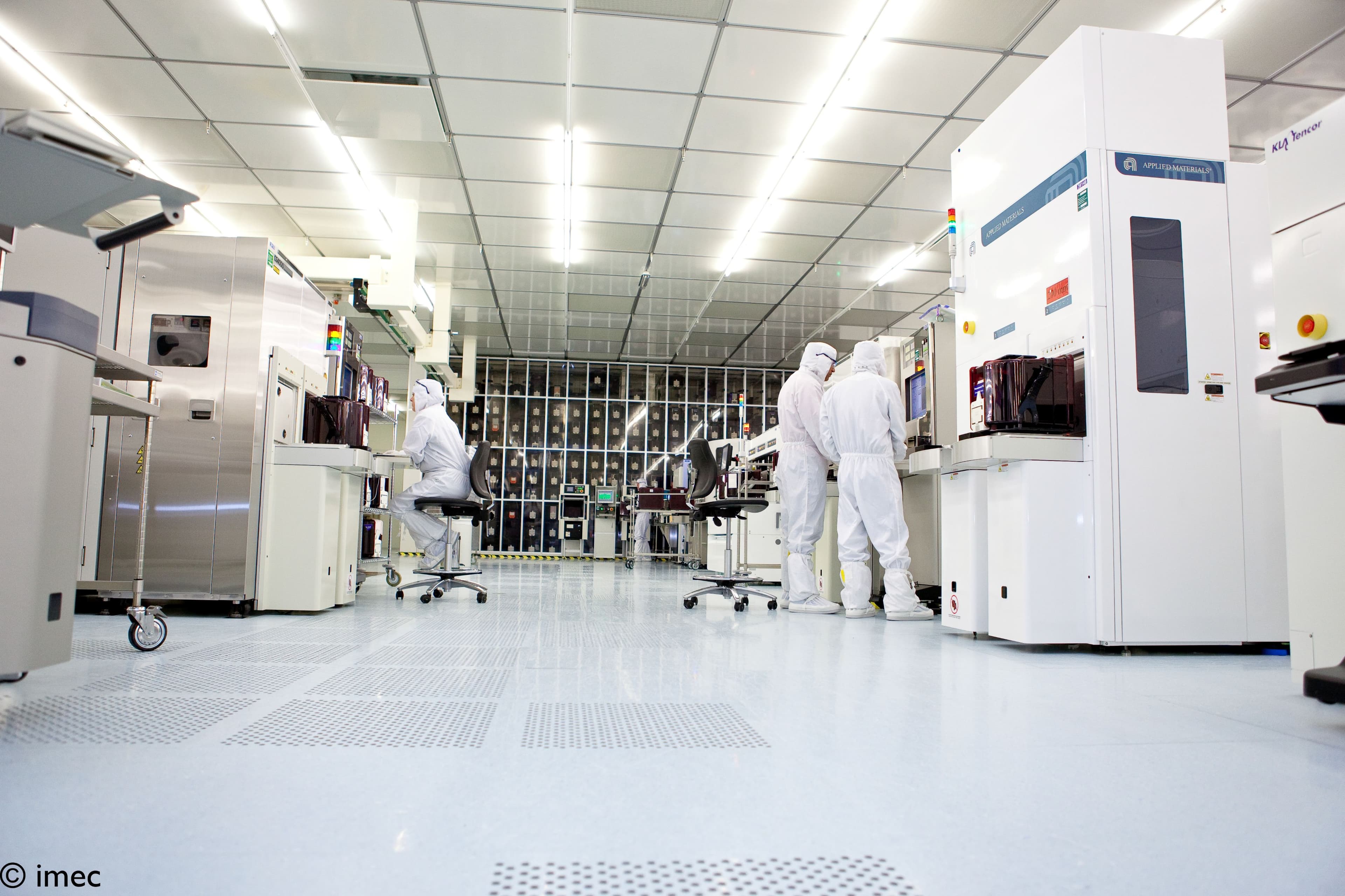
Within SSTS, imec intends to validate the source data and enrich the methods by benchmarking results from the imec.netzero platform against comparable manufacturing data from foundries and integrated device manufacturers (IDMs). Imec.netzero is a helpful tool for identifying, documenting, and classifying most high-impact problems existing in the industry. However, the industry’s voice is imperative to uncover other environmental issues that escape analysis due to their complexity, identify practical solutions to these problems, and judge their relevance/feasibility for the industry. To foster such practical solutions, imec will work with material and equipment suppliers, IDMs, and foundries to ideate industry-relevant solutions that reduce the environmental impact while keeping performance intact. In this context, the imec fab acts as a pilot environment to run some initial experiments and assess their effects.
Focus and deliverables
Close interactions with actors across the semiconductor ecosystem enable imec to detect common denominators and set priorities. Among the SSTS program's primary goals are identifying high-impact processes for logic and memory in terms of electricity consumption, greenhouse emissions, and water usage. In terms of electricity consumption, the transition to renewable energy accompanies a dedicated effort to increase the energy efficiencies of each process step and piece of machinery used. Regarding greenhouse gasses, cleaning and etching processes that use NF3, which has a 17,000 times higher global warming potential than CO2, are an obvious target. And the program looks at the bill of materials in general. As with each technology node, rare and exotic materials notorious for costing a significant amount of energy to extract from the Earth’s crust tend to enter the equation.
Identifying high-impact processes for logic and memory in terms of electricity consumption, greenhouse emissions, and water usage.
Some of the concrete program outcomes are publishing guidelines for program stakeholders, setting up a concrete roadmap for helping achieve net-zero in the industry, defining new standards for environmental assessment in the semiconductor industry, and sharing high-level learnings and data with the scientific community and broader public. However, the major challenge seems not to be technical but instead lies in the simple fact that time could be the scarcest resource of all.
Want to know more about sustainable semiconductor manufacturing?
Authors
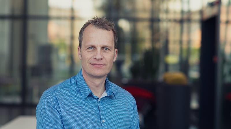
Lars-Åke Ragnarsson
Lars-Åke Ragnarsson is program director of sustainable semiconductor technologies and systems (SSTS) at imec. He received his M.S. and Ph.D. degrees in electrical engineering from the Chalmers University of Technology in Göteborg, Sweden. From 2000-2002, he did postdoctoral studies with the IBM T.J. Watson Research Center in Yorktown Heights, NY, focusing mainly on the electrical characterization of high-k dielectrics. Since 2002, he has been with imec, focusing on developing advanced technologies using high-κ dielectrics and metal gates. Today, Lars-Åke is program director in compute and memory technologies, focusing on the sustainability of current and future technologies.
Discover more





Neural telemetry breakthrough: new chip delivers ten-fold compression while preserving signal integrity
Read more
Sony and imec unveil high-density backside connectivity module enabling next-generation 3D chip integration
Read more