Navigating thermal challenges in advanced systems on chip
Thermal analysis highlights the importance of system-technology co-optimization.
In short
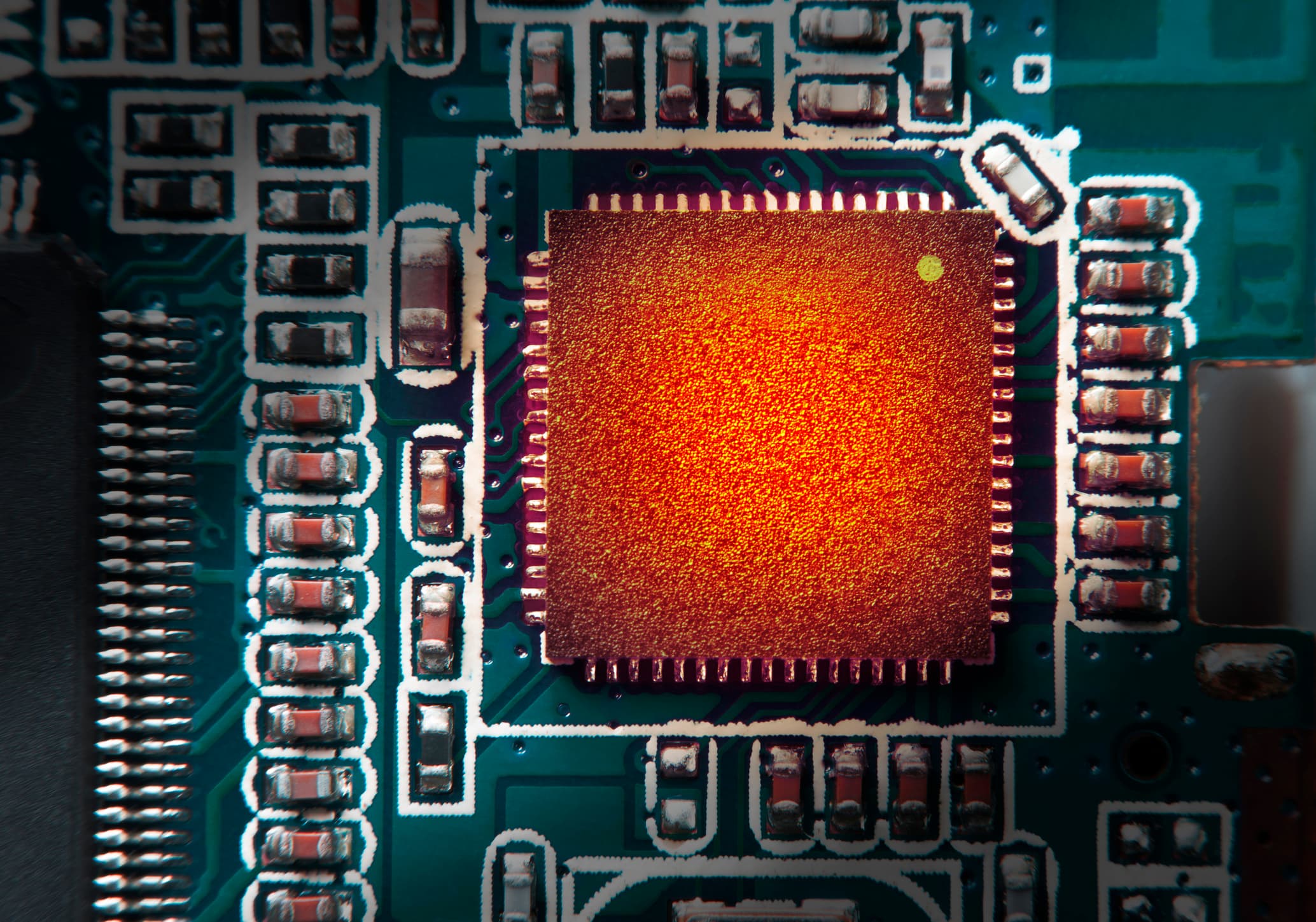
Continued transistor scaling leads to increased power densities, generating heat as a byproduct. This affects critical aspects of system on chip (SoC) performance, including processing speed, power efficiency, reliability, data throughput, and signal integrity.
This article summarizes insights from simulations based on four recent imec papers. The simulations quantify thermal challenges in advanced nodes and show why existing cooling options alone may no longer be sufficient. They also point to new design strategies, such as backside functionalization and the separation of logic layers optimising transistors for either density or drive current.
Addressing these thermal concerns effectively will require system-technology co-design, embedding thermal considerations into the earliest phases of chip and technology development.
As transistor scaling continues to push the boundaries of chip performance, it brings with it a growing thermal challenge. Higher power densities in advanced system-on-chip (SoC) architectures generate more heat, which in turn affects performance, reliability, and overall efficiency.
In this article, imec explores how these thermal issues can be tackled through a dedicated simulation framework and a forward-looking technology co-design approach.
Key takeaways include:
- Why traditional cooling methods may no longer suffice for future SoC nodes due to increased thermal dissipation.
- How imec’s simulation framework helps quantify and predict thermal hotspots in next-generation chips.
- What thermal trade-offs may be introduced by backside power delivery networks (BSPDN), including a potential ∼14°C temperature rise due to reduced lateral heat spreading.
- How the CMOS 2.0 paradigm, including splitting logic into density-optimized and drive-optimized layers, may offer thermal benefits by reducing power density.
- Why it is crucial to integrate thermal management into SoC architecture, design flow, and technology development from the outset.
The full article is available on IEEE Spectrum.
Authors

James Myers
James Myers holds a MEng degree in Electrical and Electronic Engineering from Imperial College in London. He spent 15 years at Arm, leading research from low power circuits and systems, through printed electronics, to DTCO activities. He joined imec in 2022 to lead the System Technology Co-optimization program, with the aim of building upon established DTCO practices to overcome the numerous scaling challenges foreseen for future systems. James holds 60 US patents, has taped out 20 SoCs, has presented at ISSCC and VLSI Symposium, and has published in IEDM and Nature.
Discover more





Neural telemetry breakthrough: new chip delivers ten-fold compression while preserving signal integrity
Read more
Sony and imec unveil high-density backside connectivity module enabling next-generation 3D chip integration
Read more