The potential of sequential-3D integration for advanced semiconductor scaling
Sequential-3D integration is perceived as a promising alternative to continue the benefits offered by semiconductor scaling. Nadine Collaert (distinguished member of technical staff at imec) and her team review the technology integration challenges and the potential benefits of this emerging integration technology.

Intro
Technology innovations are expected to allow traditional Moore’s Law scaling for logic and memory applications to continue for at least five to ten years. At the same time, researchers worldwide are exploring alternative options to overcome a number of challenges – physical, technological and economical – associated with further scaling of CMOS transistor dimensions. One of these alternatives is sequential-3D integration (S3D), a relatively new technology that promises to alleviate problems in classical 2D CMOS. This integration technique involves the vertical integration of sequentially processed device layers, and comes in three different flavors – depending on where the partitioning and stacking takes place.

One of these alternatives is sequential-3D integration (S3D), a relatively new technology that promises to alleviate problems in classical 2D CMOS.
Three different S3D flavors
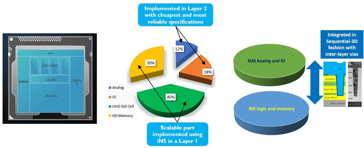
Firstly, in transistor-level S3D, the CMOS gate is split into tiers of pMOS and nMOS. Secondly, in CMOS-level S3D, conventional 2D standard cells are placed in different tiers. And finally, the partitioning can be done at IP block level to separate, for example, the analog and I/O functionality from the logic and memory part. This is referred to as hybrid S3D (or heterogeneous S3D) where besides CMOS devices, different flavors of technologies can be combined.
Sequential-3D (a) at transistor level and (b) at cell level
Technology integration challenges
S3D comes with its own set of technology challenges, mainly caused by the limited thermal budget that is available for processing the top and bottom tiers. Imec has proposed innovative solutions for processing the interconnect metals, the device contacts and gate stacks. With these solutions, the technique is expected to further enhance device density per chip area, reduce the length of the interconnection lines, and facilitate the co-integration of heterogeneous device technologies.
Potential benefits
To quantify the true benefits, the imec team has performed a systematic power-performance-area-cost analysis for each of the S3D flavors.
As a main conclusion, the largest benefit is found for a heterogeneous S3D case, where the logic and memory part is using a scaled technology, and the remaining non-scalable part (analog in combination with I/O) is manufactured in a more relaxed 28nm technology in the top tier.
S3D is found to be less straightforward for dimensional scaling (i.e., S3D at transistor or cell level). The relative benefits are however largely dependent on the technology assumptions and on the component distribution.
A typical application of a S3D implementation can be stacked SRAM cells, where transistors of neighboring cells are stacked on top of each other. The hybrid S3D approach will e.g. benefit the implementation of next-generation application hardware such as 5G and machine learning.
Want to know more?
- An extended version of this article was originally published in Chip Scale Review (May-June 2018), and can be requested via this link. The article is entitled ‘Sequential-3D integration for advanced semiconductor scaling’, and is authored by Anne Vandooren, Jacopo Franco, Arindam Mallik, Liesbeth Witters and Nadine Collaert, imec, Leuven, Belgium.
Authors
Nadine Collaert
Nadine Collaert is program director at imec and responsible for the High-speed analog/RF program. She received an M.S. and Ph.D. degree in electrical engineering from the ESAT Department, KU Leuven, Belgium, in 1995 and 2000, respectively. Since then, she has been involved in the theory, design and technology of FinFET devices, emerging memory devices, transducers for biomedical applications and the heterogeneous integration of new materials with Si.
Discover more



Imec and Diraq demonstrate first coherent operation of eight silicon MOS spin qubits fabricated in a 300mm CMOS-compatible foundry process
Read more


Neural telemetry breakthrough: new chip delivers ten-fold compression while preserving signal integrity
Read more

