Paul Heremans on thin-film technology
“Our experts are working on what will be the next revolution in consumer electronics”
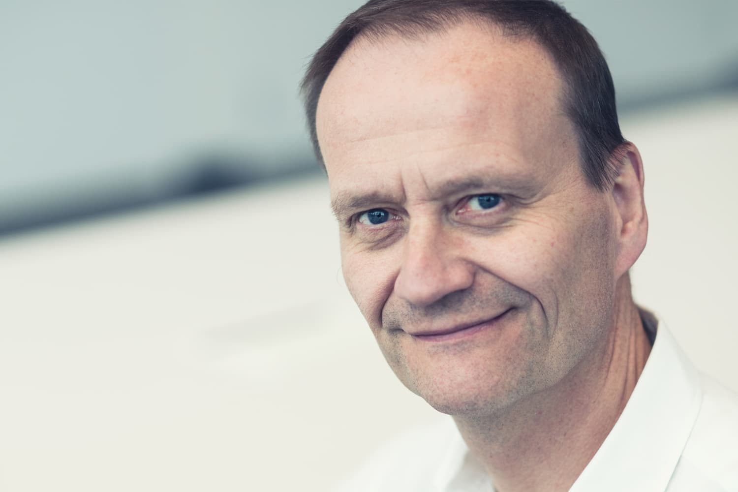
Paul Heremans, imec fellow & expert in thin-film electronics
Books with moving images, curtains that give off light, glasses that show us what we aren’t able to see with our eyes, 3D images with a feel ... These are applications that appeal to our imagination but that we’ve so far only encountered in fantasy and science-fiction. However, there is a promising technology – thin-film electronics – in which we might actually create these wonders for real. The first prototypes and products are already here, but there is still a long way to go before we can profit from the full potential of this technology. Imec’s scientists are at the cutting edge of research and together we are working on the next revolution in consumer electronics.
Thin-film electronics are created by applying thin layers of suitable materials onto flexible carriers such as plastic films. In contrast to silicon chip manufacturing, this process has fewer steps and can be done on larger surfaces and at a lower temperature, so it has the potential to be considerably cheaper. What also makes flexible electronics promising is that we will soon be able to integrate it directly into smart applications with random, flexible shapes. This will bring us lots of new and unusual products, such as smart body plasters, informative packaging or flexible displays.
In fact, this last application – the display – is one of the first successful commercial applications of thin-film technology. These AMOLED (active-matrix organic light-emitting diode) displays are made up of an active matrix of organic pixels, tiny LED lamps made from organic, printable materials that light up when power is applied. This matrix sits on top of a second matrix of thin-film transistors that function as switches to turn the pixels on and off.
Until not so long ago, most mobile phones and smart watches still had LCD displays. But recently, AMOLED displays have started gaining track. The rivalry between the two technologies long seemed undecided, but because AMOLED displays are super-thin and can be produced in a curved shape, they finally appear to be gaining the upper hand.
We expect to see the first foldaway display used in a product in 2018 – most probably in a smartphone. It has been talked about for years and the various manufacturers have demonstrated dozens of prototypes, but the challenge of incorporating such a fragile screen into a consumer product has always been too great. Now it appears the technology is finally ready.

If we look further down the line, I expect a great deal from augmented reality – with products in which we can give the user an adjusted, enhanced look on the world.
Think for example about images that reveal colors that human eyes normally cannot see, such as hues of infrared or ultraviolet. Or images to which we add smart information. Finally, we will also be able to display 3D images and, ultimately, even holographic video, enabling us to talk naturally with people who aren’t with us in the room.
Imec is doing groundbreaking work in the run-up to these applications. The importance and extent of our work is witnessed by the many publications of our scientists and by the prestigious European ERC grants that some of them have been awarded – as well as the collaborative arrangements we have with leading companies. Together we are looking for solutions that enable more and more practical applications.
Our major aim now is to reduce the power consumption of our thin-film electronics, especially the displays. At the same time we are also making great progress toward increasing the resolution and speed of these displays. Both will be necessary if we want users to be able to enjoy good-quality augmented reality.
We are also working to incorporate sensors and actuators into the displays. Our aim is to make screens smarter and get them to interact with more of our senses. We will soon be giving the first demonstration of haptic perception: by incorporating actuators that transmit ultrasonic pressure waves, we can generate tangible shapes on top of a display. That way users will not only see a push-button on the screen, but will also feel it. Which means we will be able, for example, to create e-readers for blind people, where the text is converted into tactile Braille script.
A significant part of our research consists of looking for new materials and combinations of materials that are suitable for producing increasingly fast, small and cheap thin-film transistors and circuits. The material we are using at the moment for transistors is an n-type material, a material with an abundance of electrons. We are still searching for an equivalent p-type material (with a shortage of electrons). The combination of p- and n-type transistors would allow for faster, more energy-efficient circuits. In addition, we are also constantly looking for better materials to produce the new sensors and actuators that we envisage.
Taken together, this will create nothing less than a new revolution, with a new form of electronics that is both cheaper and that can be used in a much more flexible way.
Want to know more?
- See this press release to learn more about developments on OLED displays.
- In this press release, we communicate our latest developments on 12-bit plastic RFID tags.
- And this article explains how we use near-field communication (NFC) to have playing cards communicate with a smartphone.
- See here for videos on the ERC grants of Paul Heremans and Kris Myny.
- Watch this animation on Gesture recognition and haptic feedback
Authors

Paul Heremans
Paul Heremans is an imec fellow and professor at the Electrical Engineering Department of the KU Leuven (Belgium). He is director of imec’s large area electronics department, a research activity that he started in 1998. Paul received his PhD degree in Electrical Engineering from the KU Leuven in 1990. His research interests span AMOLED displays, large-area and flexible imagers, thin-film circuits such as NFC tags, photodetectors, and polymer ultrasound transducers.
Discover more



Imec and Diraq demonstrate first coherent operation of eight silicon MOS spin qubits fabricated in a 300mm CMOS-compatible foundry process
Read more


Neural telemetry breakthrough: new chip delivers ten-fold compression while preserving signal integrity
Read more

