CPT and imec / Holst Centre Demonstrate 1250 ppi, FMM-free Multicolor OLED Displays with Photolithography
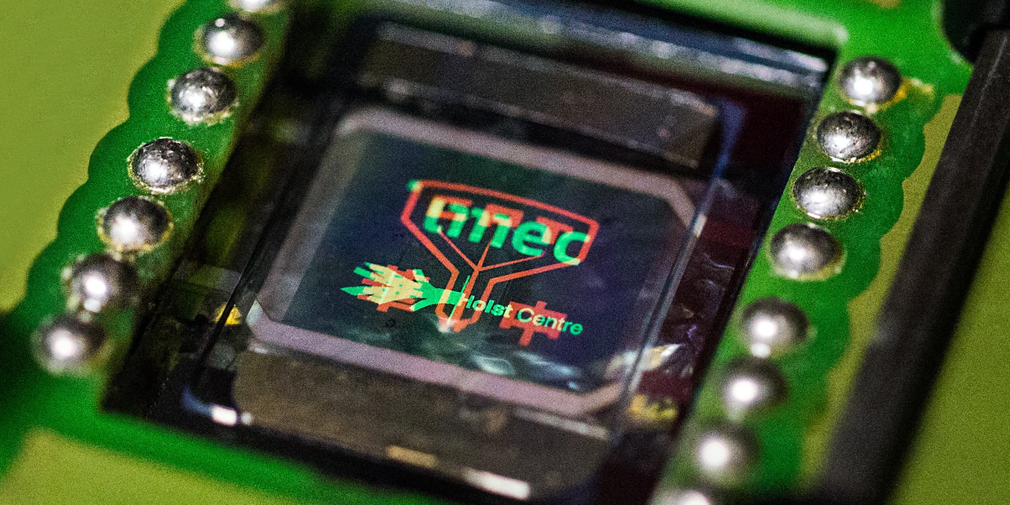
Taipei, Taiwan ROC, September 20, 2017– Chunghwa Picture Tubes Ltd. (CPT) together with the European research institute imec in the framework of the Holst Centre collaboration, showcase today an ultra-high resolution display realized by photolithography patterning of organic light emitting diode (OLED) arrays. The results pave the way to cost-effective manufacturing of fine, side-by-side pixels in OLEDs, and will be presented at the annual International Smart Display and Touch Panel Exhibition, Touch Taiwan, in Taipei, Taiwan ROC, Sep 20 – Sep 22.
High quality displays are at the core of modern, connected society, with mobile screens enabling and enhancing an ever-increasing number of daily appliances. Active-matrix organic light-emitting diode (AMOLED) displays, with discrete light emitting pixels, are steadily growing, not only in market share, but also in achievable resolution, brightness, size and lifetime. To continue the advancement of this technology, imec together with its program partners are researching a cost-effective manufacturing method for OLED arrays featuring fine pixels. Pushing the pixel density beyond 1000 ppi is a necessary step for implementation of next-generation displays, especially for virtual and augmented reality.
CPT and imec have verified that a novel photolithography process can allow for ultrafine OLED patterns. The proposed technique does not require using fine-metal masks to structure thermally evaporated OLED stacks (“FMM-free”). One of the main challenges when applying standard photolithography is the fragility of the organic materials for the photolithography chemicals. To circumvent this issue, imec and CPT have used an i-line, chemically amplified photoresist system in a process flow dedicated to OLED stacks. Apart from ultra-high resolution, other benefits of photolithography include high aperture ratio, large substrate size compatibility and good yield control.
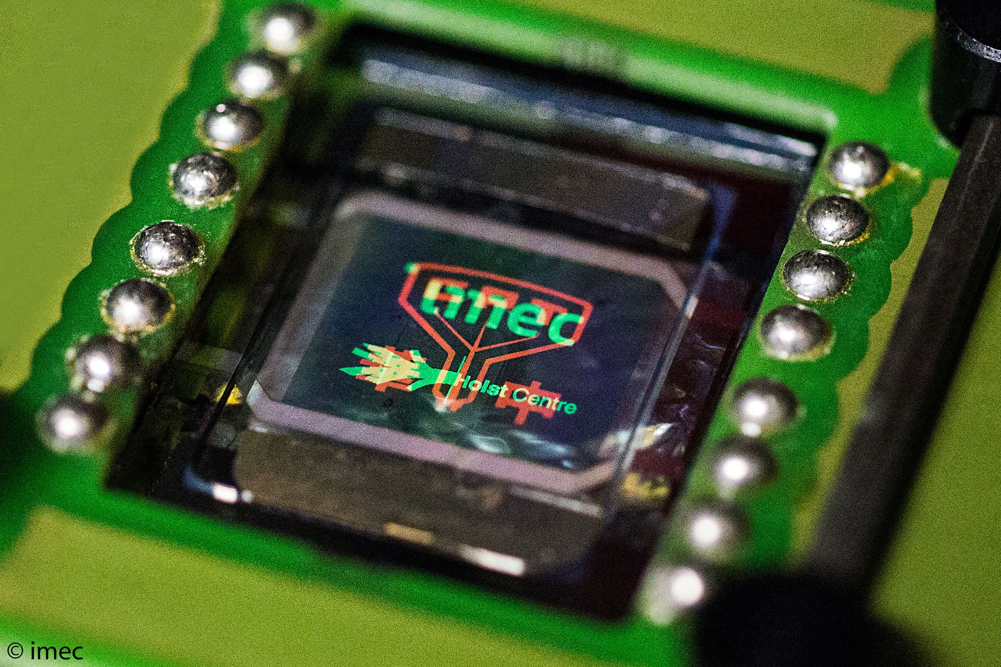
The proof-of-concept is a passive display with 1400x1400 pixels (1.96 megapixel) of side-by-side, orange and green OLEDs. The sub-pixel pitch of 10 μm results in the equivalent resolution of 1250 ppi. Uniform electroluminescence is demonstrated with the possibility to light up each color separately. Moreover, preliminary lifetime investigation shows operation of each color after patterning for a few hundred hours at more than 50% of the original brightness.
“Our goal is to identify and explore technology bottlenecks in the extremely competitive and fast-paced display industry. With research activities spanning from material and device science, through design, fabrication and integration all the way to tech transfer, we make use of our semiconductor and thin-film background,” stated Paul Heremans, program director of thin-film electronics at Holst Centre/imec. ”The collaboration with CPT enables us to improve the manufacturability readiness level of the OLED photolithography patterning method. This will enable production of ultra-high resolution OLED displays for next-generation user interfaces. We are very happy to have the possibility to explore this exciting technology route with our innovative partners.”
--end--
* OLED: Organic Light-Emitting Diode. Light-emitting elements using organic semiconductors, used for organic EL displays' pixels
** Photoresist: Photosensitive materials that cause photochemical reaction due to light exposure, have different developer solubility at exposed parts and unexposed parts, and are used for microfabrication in semiconductor production.
*** Micron: 1/1000 mm.
*4 ppi: Pixels per inch. A unit of pixel density for information displays. It refers to the number of pixels in one inch.
*5 Photolithography method: A film is formed by coating photoresist onto the substrate to be processed, and photochemical reaction occurs within the resist film by exposing patterns through the mask. This microfabrication method forms a mask-like resist pattern on the substrate through development, and transfers the resist pattern onto the substrate as protective material for etching.
*6 Subpixel pitch: Subpixel refers to pixel (red, green, blue, etc.) of the smallest unit. Subpixel pitch represents the midpoint distance between two neighboring subpixels.
*7 Passive display: Display with a fixed pattern that can be switched on and off. There is no backplane for individual driving of the OLED pixel array.
About imec
Imec is the world-leading research and innovation hub in nanoelectronics and digital technologies. The combination of our widely acclaimed leadership in microchip technology and profound software and ICT expertise is what makes us unique. By leveraging our world-class infrastructure and local and global ecosystem of partners across a multitude of industries, we create groundbreaking innovation in application domains such as healthcare, smart cities and mobility, logistics and manufacturing, energy and education.
As a trusted partner for companies, start-ups and universities we bring together close to 3,500 brilliant minds from over 75 nationalities. Imec is headquartered in Leuven, Belgium and also has distributed R&D groups at a number of Flemish universities, in the Netherlands, Taiwan, USA, China, and offices in India and Japan. In 2016, imec's revenue (P&L) totaled 496 million euro. Further information on imec can be found at www.imec-int.com.
Imec is a registered trademark for the activities of IMEC International (a legal entity set up under Belgian law as a "stichting van openbaar nut”), imec Belgium (IMEC vzw supported by the Flemish Government), imec the Netherlands (Stichting IMEC Nederland, part of Holst Centre which is supported by the Dutch Government), imec Taiwan (IMEC Taiwan Co.) and imec China (IMEC Microelectronics (Shanghai) Co. Ltd.) and imec India (Imec India Private Limited), imec Florida (IMEC USA nanoelectronics design center).
About Holst Centre
Holst Centre is an independent R&D center that develops technologies for wireless autonomous sensor technologies and for flexible electronics, in an open innovation setting and in dedicated research trajectories. A key feature of Holst Centre is its partnership model with industry and academia based around shared roadmaps and programs. It is this kind of cross-fertilization that enables Holst Centre to tune its scientific strategy to industrial needs.
Holst Centre was set up in 2005 by imec (Flanders, Belgium) and TNO (The Netherlands) and is supported by local, regional and national governments.
Located on High Tech Campus Eindhoven, Holst Centre benefits from, and contributes to, the state-of-the-art on-site facilities. Holst Centre has over 200 employees from some 28 nations and a commitment from over 50 industrial partners.
Contact
Hanne Degans, press communications manager, T: +32 16 28 17 69 M: +32 486 065 175, Hanne.Degans@imec.be
Discover more


Imec and Diraq demonstrate first coherent operation of eight silicon MOS spin qubits fabricated in a 300mm CMOS-compatible foundry process
Read more


Neural telemetry breakthrough: new chip delivers ten-fold compression while preserving signal integrity
Read more