In pursuit of high-density storage class memory
A novel thermally stable GeSe-based selector paves the way to storage class memory applications.

Intro
The existing memory hierarchy in computer systems can be further improved by adding a new memory class that fills the DRAM-NAND gap: storage class memory. Densely packed resistive RAM (RRAM) arrays – an emerging memory based on resistive switching – is a promising candidate to help fill this gap. But so far, the implementation of high-density RRAM lags behind. One of the important reasons were sneak current issues in the high density 4F2 architecture. One way to suppress this parasitic leakage is to add a so-called two-terminal selector that connects serially with each resistive memory element in a 4F2 configuration. At VLSI 2017, imec proposed a novel selenium (Se)-based selector that displays characteristics closely compliant with the required two-terminal selector for storage class memory application. In this article, Gouri Sankar Kar, Distinguished Member of Technical Staff at imec, discusses the challenges for implementing a selection device, and highlights the importance of imec’s new thermally stable germanium-selenium (GeSe)-based selector.
Storage class memory: filling the gap between DRAM and NAND Flash
The future memory landscape requires a new class of memory that is able to fill the gap between dynamic random access memory (DRAM) and NAND Flash memories in terms of density, cost and performance: the storage class memory. This new memory class should allow massive amounts of data to be accessed in a very short time. Gouri Sankar Kar: “Most probably, more than one novel memory technology will be required to span the entire gap."

"One of the candidates that could potentially fill the gap towards the DRAM side, is resistive random access memory (RRAM) – which promises near-DRAM performance, but with higher density and at a lower cost.”
A RRAM memory cell typically consists of a two-terminal element with top and bottom electrodes that sandwich a thin dielectric layer. By applying a voltage across the electrodes, the electrical conductivity of the dielectric can be reversibly changed, from a low-resistance state (LRS) to a high resistance state (HRS) or vice versa. In most of the RRAM devices, this resistive switching is based on the formation of a conductive filament in the insulating layer.
The need for a non-linear selection device
To exploit the potential of RRAM as a high-density memory technology, the memory cells are typically packed in so-called cross-point arrays. Cross-point arrays generally include bit lines (BL, arranged in columns), word lines (WL, arranged in rows) and memory cells located at the intersection (or cross point) of each bit and word line. In this configuration, the effective cell area is as small as 4F2, with F being the technology node’s feature size (i.e., the half-metal pitch in memory technology). Gouri Sankar Kar: “In the ideal case, reading or writing a memory cell is supposed to take place only on the selected cell, leaving the rest of the cells unaffected. In reality, however, sneak currents run through the unselected cells in the cross-point array during memory operation, degrading the selectivity of the memory cell and leading to incorrect information retrieval. These sneak currents mainly occur because of the nearly linear (Ohmic) I-V behavior of the resistive memory cells in both the low and high resistive state.”
"An attractive approach to suppress the sneak currents is to add an additional ‘selection’ device, called the selector, having non-linear I-V characteristics and connecting serially with each resistive memory element in a one-selector one-resistor (1S1R) configuration."
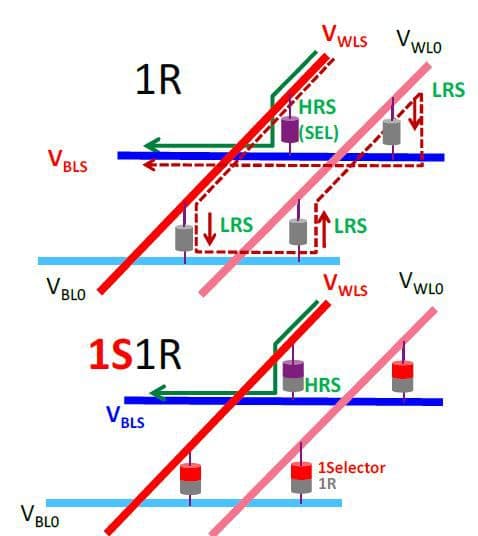
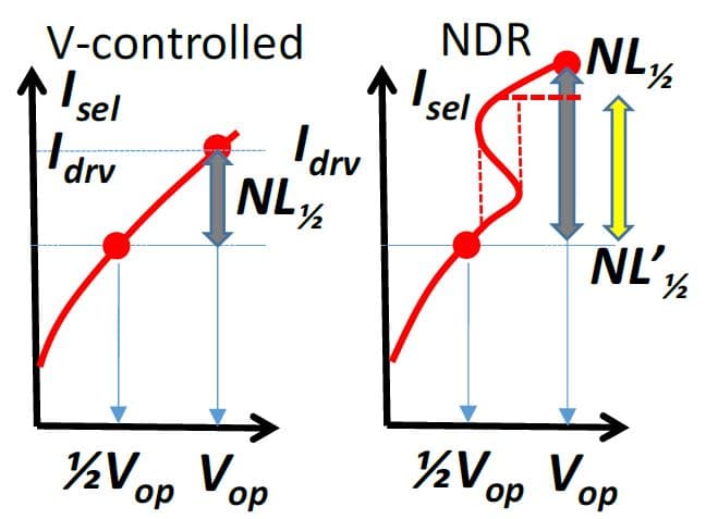
“In order to meet the specs for storage class memory operation, the selectors are subject to stringent requirements,” says Gouri Sankar Kar. “For example, for high-density applications, a two-terminal selector is preferred – as it consumes the least possible memory array area. Also, the selector should have a high drive current, in order to provide the current needed to transition between the resistive states of the memory cell. And it should operate at a speed compatible with the high switching speed of the memory cell. Other important characteristics are a high (half bias) non-linearity factor for enhanced cell selectivity, a low leakage current, and a good program/erase cycle endurance – as good or even better than the resistive memory cell itself. Finally, the fabrication process must be compatible with CMOS processing, and the selector needs to be thermally stable to enable processing of subsequent memory layers that sit on top of the selector device.”
Selector candidates
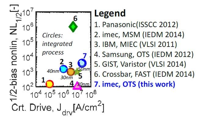
Various kinds of two-terminal selector devices have been extensively studied in order to obtain the best performance cross-point memory arrays. Si-based selectors, pn and Schottky diodes, mixed ionic electronic conductor (or MIEC) selectors and volatile conducting bridge (or VCB) selectors are just a few examples. “At this stage, none of these selectors has the desired characteristics, and come with numerous trade-offs that have to be made,” remarks Gouri Sankar Kar. “A pn diode, for example, is a unipolar device. But due to the fact that most of the resistive memories operate in bipolar switching mode, a bipolar selector device is required. Other selector candidates may exhibit good characteristics, but lack e.g. the required high current density.”

Recently, ovonic threshold switching (or OTS) devices have received much attention, as they promise full cell selectivity (a high non-linearity factor), low leakage current and high drive currents.
Ovonic threshold switching refers to the rapid increase of current, observed in the I-V characteristics of various amorphous chalcogenide materials during voltage sweep. OTS devices therefore typically contain an amorphous chalcogenide material sandwiched between two metal electrodes. Gouri Sankar Kar: “Yet, a major weakness of this selector type is the thermal budget. For most of the chalcogenide materials researched so far, the thermal budget stays below 300°C, which is too low for subsequent processing of the resistive memory element.”
Imec’s solution: a thermally stable GeSe-based OTS selector
According to Gouri Sankar Kar, the imec team has screened a variety of chalcogenide materials.
“This has resulted in a novel GeSe-based OTS device that fullfulls all the requirements imposed by future high-density storage class memories."
"The devices show record 23MA/cm2 drive current density and good half-bias non-linearity (about 3500). The selector devices are thermally stable at 350°C, and withstand 108 program/erase endurance cycles.”
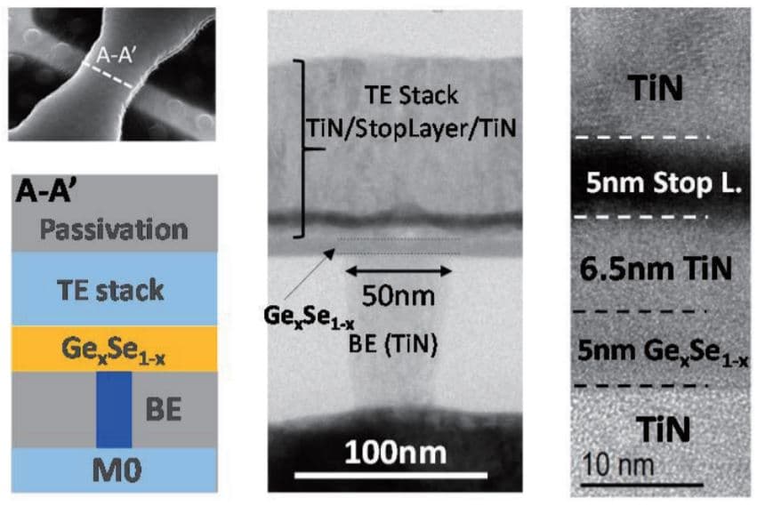
Key to these results is a unique GeSe film composition. For example, the high thermal stability has been obtained after dopant optimization, and the electrical properties of the selector device are tunable by careful control of the film composition and thickness.
The GeSe films have been deposited by physical vapor deposition (PVD), with film thicknesses down to 5nm. The overall size of the TiN/GeSe/TiN selector device is as small as 50nm.
Towards true 3D storage class memory
In the longer term, storage class memory will eventually evolve into a 3D configuration, and this involves two possible integration routes. One route consists of simply stacking the 2D planar RRAM layers on top of each other. Gouri Sankar Kar: “This route has two main drawbacks. Firstly, it does not save any litho or mask steps. On the contrary, expensive litho steps in combination with e.g. self-aligned double patterning schemes are required to stack the layers, and this significantly adds to the cost of the 3D memory. Secondly, the scalability of this stacked configuration is challenging. For example, when scaling down the resistive memory element, the drive current does not scale down accordingly. This means that also the current density of the scaled selector devices increases dramatically. As a consequence, with further scaling, a new generation of selector materials will be required allowing for higher current densities. Also, increased WL and BL resistances add an additional performance penalty as scaling continues.”
"Alternatively, the imec team is exploring a true 3D integration route. This involves the deposition of multiple selector-resistor stacks sequentially, without requiring litho steps in between."
In this configuration, density is not defined by the critical line critical dimensions (CDs), leading to relaxed CDs, and allowing the same generation of selector materials for different scaling nodes. “This innovative 3D technology comes with its own unique challenges”, says Gouri Sankar Kar. “For example, a uniform deposition of the chalcogenide material in the new structure is no longer possible by using conventional PVD. Instead, alternative deposition processes such as atomic layer depostion (ALD) should be used. Therefore, imec, in collaboration with equipment and materials suppliers, is currently developing a reliable ALD chalcogenide process – an essential step in the realization of a future, truly 3D storage class memory.”
Want to know more?
Send an e-mail to imecmagazine@imec.be to receive the articles below:
- 'Thermally stable integrated Se-based OTS selectors with >20 MA/cm2 current device, >3.103 half-bias nonlinearity, tunable threshold voltage and excellent endurance’, B. Govoreanu et al, VLSI 2017
- ‘Doped GeSe materials for selector applications’, N.S. Avasarala et al., ESSDERC-ESSCIRC 2017
Authors

Gouri Sankar Kar
Gouri Sankar Kar received the PhD degree in semiconductor device physics from the Indian Institute of Technology, Khragput, India in 2002. From 2002 to 2005, he was a visiting scientist at Max Planck Institute for Solid State Research, Stuttgart, Germany, where he worked with Nobel Laureate (1985, Quantum Hall Effect) Prof. Klaus von Klitzing on quantum dot FET. In 2006, he joined Infineon/Qimonda in Dresden, Germany as lead integration engineer. There he worked on the vertical transistor for DRAM application. In 2009, he joined imec, Leuven, Belgium, where he is currently distinguished member of technical staff (DMTS). In this role, he defines the strategy and vision for RRAM, DRAM-MIMCAP and STT-MRAM programs both for stand-alone and embedded applications.
Discover more



Imec and Diraq demonstrate first coherent operation of eight silicon MOS spin qubits fabricated in a 300mm CMOS-compatible foundry process
Read more


Neural telemetry breakthrough: new chip delivers ten-fold compression while preserving signal integrity
Read more

