Enhancing efficiency and stability of Perovskite solar cells
Molecular interface engineering: a pathway to scalable manufacturing
In short
Metal halide perovskites show great promise for next-generation photovoltaic cells. However, commercialization requires industry-compatible processing techniques to address stability issues.
The largest efficiency losses and instability of perovskite solar cells are reported at the interfaces between the perovskite absorber and charge transport layers.
In this article, dr. Tom Aernouts presents an ammonium salt treatment to enhance two critical interfaces, creating highly efficient, stable, and scalable perovskite cells.
Emergence of Metal Halide Perovskites in PV cells
Due to their extraordinary optical and electronic properties, metal halide perovskites have emerged as highly promising materials for next-generation photovoltaic (PV) cells. This is best illustrated by the rapid improvement in PCE, a performance measure, of perovskite solar cells from <4 percent to >20 percent in a matter of years. However, commercialization of such applications requires industry-compatible processing techniques, which overcome current stability issues, amongst others.
The largest PCE losses and instability of perovskite solar cells (PSCs) are widely reported at the interfaces between the perovskite absorber and charge transport layers. These transport layers are crucial for facilitating the efficient extraction and transport of charge carriers. Optimization of these interfaces can consequently minimize losses and improve energy extraction, resulting in increased device efficiency and operational stability.
Enhancing efficiency and stability
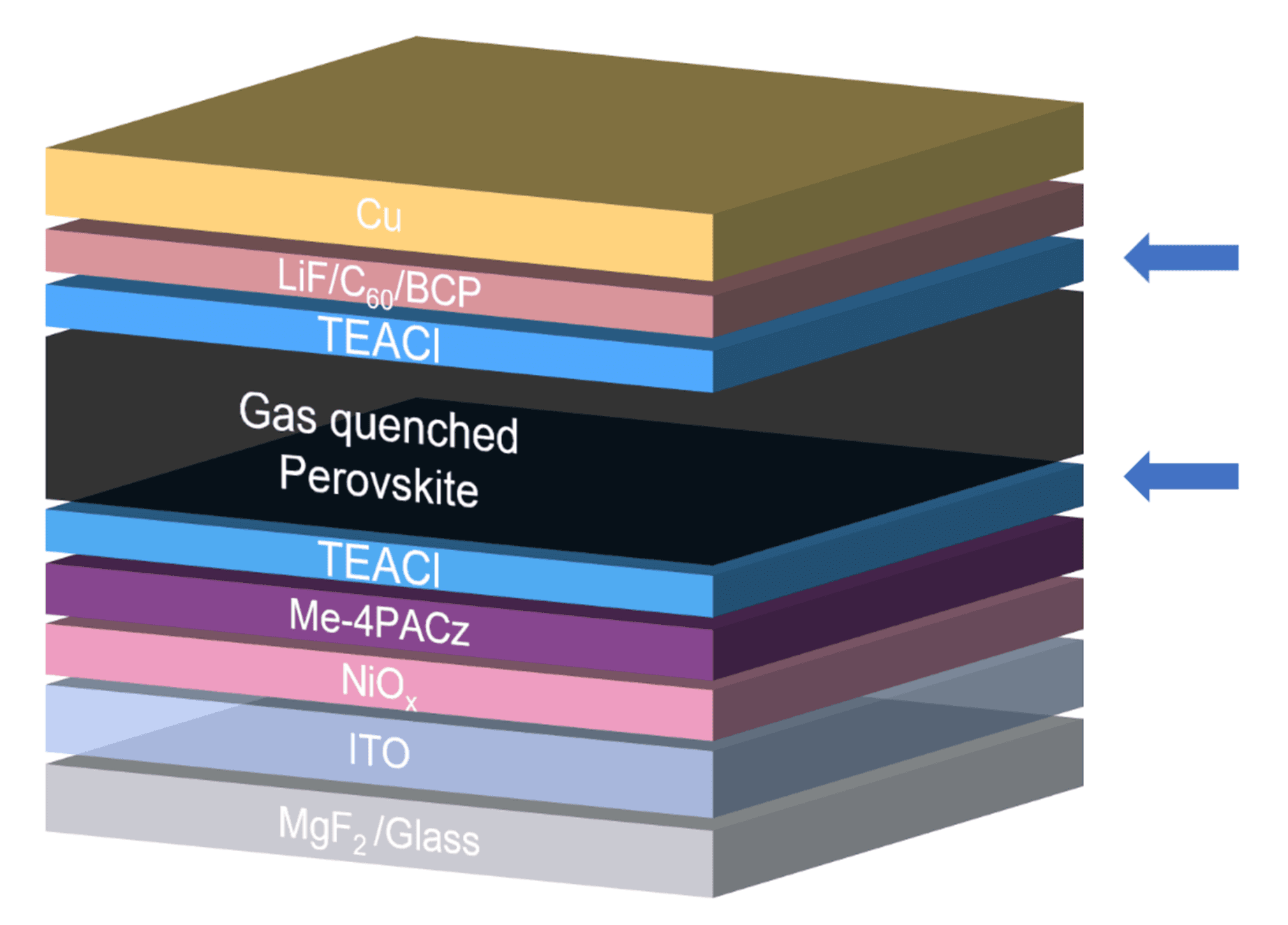
A research collaboration between imec and UHasselt at Energyville, Belgium, focused on improving the two perovskite interfaces: the ‘upper’ interface (between the perovskite and the fullerene-C60 electron transport layer) and the ‘lower’ interface (between the perovskite and the NiOx-based hole transport layer).
To enhance efficiency, both interfaces were treated with an ammonium salt, specifically 2-thiopheneethylammonium chloride (TEACl). The results were compared to PSCs with untreated layers. Said treatment is expected to increase performance by creating a 2D perovskite layer at the interface.
The resulting upper and dual-interface-treated perovskite solar cells exhibited suppressed nonradiative recombination, improved interfacial contact, and optimized band alignment compared to both controls. Specifically, a champion PCE of 24.3 percent was achieved for the dual-interface-treated solar cells, along with a short-circuit density of 24.5 mA/cm2, an open-circuit voltage of 1.17 V, and a fill factor of 84.6 percent.
“Besides the increase in efficiency, we also observed a remarkable stability,” stated Tom Aernouts, R&D manager of the Thin-Film Photovoltaics team. Indeed, after 1,000 hours of continuous operation under one-sun illumination, the devices showed a 97 percent retention of performance, which is among the current bests. Moreover, after 1,850 hours of aging, dual-layer-treated cells retained 88 percent of their initial performance, compared to 55% in non-treated cells. Combined, these results demonstrate extraordinary operational and thermal stability of the treated PSCs.
Upscaling to a mini-module
Next to cell-level optimizations, researchers also examined further upscaling to a mini-module with an active area of 3.63 cm2. “Our research group aims not only to develop more efficient but also scalable PSCs, paving the way for commercialization. Therefore, at the PV cell production level, materials and processes are chosen and evaluated based on these future perspectives.” A high PCE of 22.6 percent and a fill factor of 82.4 percent were maintained in the mini-module with interface treatment, indicating excellent reproducibility.
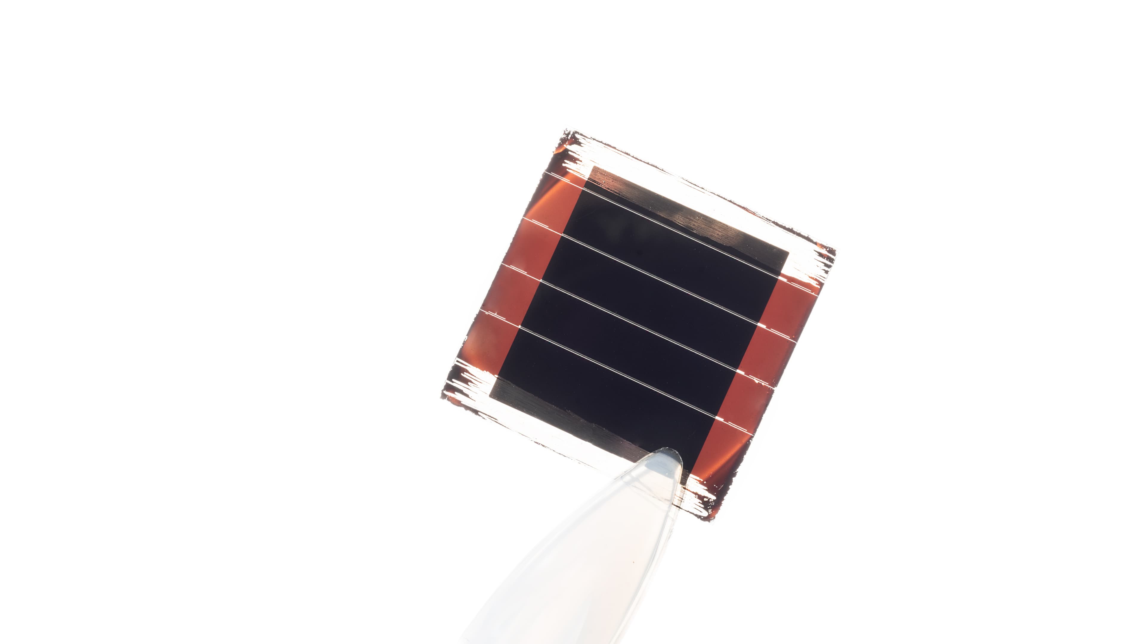
The modification strategy, which resulted in highly efficient, stable, and scalable perovskite cells, provides opportunities for a wide range of compositions and other device architectures, such as tandem cells. “Since dual interface modulations have shown effectiveness in different perovskite compositions, these findings further contribute to the development of scalable and commercially viable perovskite solar cell technology,” conclude the researchers.
The findings are described in full in the article ‘Minimizing the Interface-Driven Losses in Inverted Perovskite Solar Cells and Modules,’ which can be found in ACS Energy Letters.
Authors

Tom Aernouts
Dr. Tom Aernouts received his M.Sc. in semiconductor physics in 1998, and a Ph.D. in Science in 2006, both from the KU Leuven, Belgium. He initiated the research on thin-film solar cells at imec in 1999. Working on the fundamental understanding of organic solar cells and developing bulk heterojunction solar cells and fully flexible modules until 2006, Tom has since led imec’s thin-film PV group, steering imec’s thin-film PV research activities. The group expanded its activities in 2014 with the work on hybrid, perovskite-based thin-film solar cells and in 2018, with the move to EnergyVille, extended the device size to 35x35cm². As of October 2021, Dr. Aernouts leads the merger of thin-film PV activities at imec and imo-imomec/EnergyVille, broadening the activity into CIGS, Kesterites and other novel material systems.