Developing silicon photonics technologies with a wafer-level test station
Imec and FormFactor present a unique wafer-level test solution that enables semi-automatic testing of passive and active silicon photonics components and circuits.

Intro
The compute power of logic chips and the storage capacity of memory chips have scaled exponentially over the past few decades. As a result, the demand for input/output (I/O) bandwidth has followed a similar trend, now requiring terabyte-per-second I/O aggregate bandwidth at chip level. Silicon (Si) photonics is a promising technology to deliver such massive I/O bandwidth, especially for applications that require long interconnect distances. With Si technology, high-performance optical transceivers can be fabricated, combining passive components (such as waveguides and optical filters) and active devices (such as photodiodes and modulators) on a single silicon wafer.
The economic viability of the optical interconnects largely depends on the cost of the optical transceiver. The use of Si photonics provides a path to reduce the fabrication cost of the photonics components, as existing CMOS infrastructure and processing techniques can be leveraged. Yet, like all micro-electronic products, optical transceivers need to be tested for manufacturing defects before they can be shipped with acceptable quality levels to customers.
Testing the active and passive components of integrated Si photonics circuits contributes significantly to the cost of optical links. Typically, manufacturing tests already are performed at wafer level to prevent packaging costs for known-bad devices, as packaging also is expensive. With Si photonics in the technology development phase, these tests have been performed with manual test stations. But, now that the volume of optical I/O devices is picking up, (semi-)automated wafer-level test stations are needed to accelerate the development and production of optical links.
To illustrate the need for such (semi-)automated test stations, we use imec’s Si photonics platform as an example. Targeting the telecom and datacom industries, it co-integrates a variety of passive and active components. Besides developing specific process modules, imec has established a library with standard components. But ensuring predictable, stable, reliable, and cost-efficient library components requires efficient, automated wafer-level testing capabilities that provide accurate and fast feedback on the device performance to process engineers, as well as optical component and circuit designers.
A flexible test setup
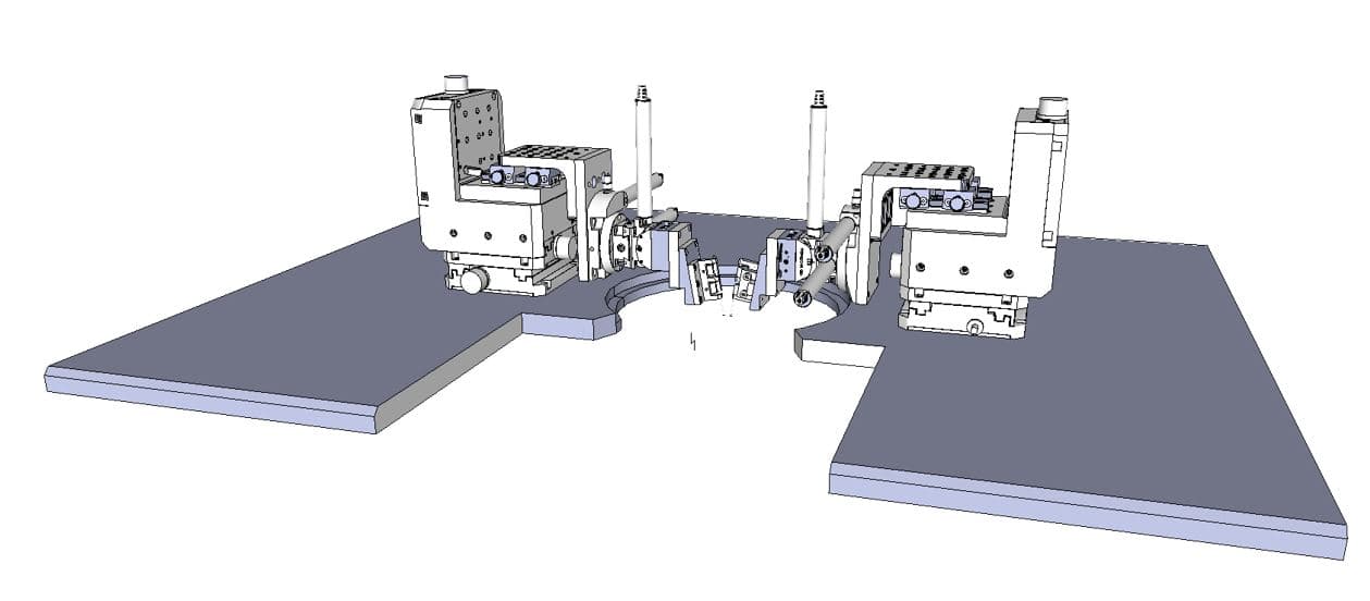
Imec and FormFactor have developed a photonics test station that allows characterizing both passive and active Si photonics devices at wafer level (both 200mm and 300mm wafers), in a semi-automatic way. In a semi-automatic test station, a single wafer is manually loaded, after which the prober automatically steps over the wafer.
The system is built around FormFactor’s Cascade PA300 semi-automatic ø300mm probe station, equipped with an RF probe manipulator and two motorized fiber manipulators. These fiber manipulators allow the measurement of any combination of optical and electrical ports within photonic circuits. For passive devices (such as fiber-grating couplers, waveguides, and filters), the optical transmission spectrum can be measured. For active devices (such as photodiodes and modulators), electrical (at DC and RF frequencies) and electro-optical parameters can be measured.
Challenges developing a photonics wafer probe station
The development of wafer-level photonics test hardware is an emerging application for test equipment manufacturers and comes with its own set of challenges.
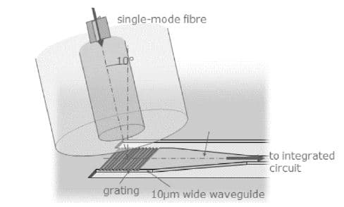
First, optical testing at wafer level requires a method for efficiently coupling light from, for example, a single-mode optical fiber into the optical circuits on the wafer. A well-known approach is to use fiber-grating couplers, which allow out-of-plane optical coupling between the waveguide on the wafer and the single-mode fiber. To minimize coupling variability, a precise and robust alignment step of the fiber to the fiber-grating coupler is required prior to each measurement. Second, the topography of the chuck that holds the wafer during testing is important, as any non-planarity can affect the measurements results.
Finally, coping with unwanted fluctuations and obtaining high quality, consistent data sets from wafer-to-wafer (or from lot to lot) is a major concern. The data can easily be influenced by a change in polarization of the incoming light (caused by movement of the optical fiber), or by a change in insertion loss (or signal power) at the optical fiber connectors. Therefore, monitoring and ensuring the short-term repeatability and long-term reproducibility of the measurement results is a key requirement.
Coupling light into optical circuits
The team made use of single-mode fibers and fiber-grating couplers to couple light from the optical fiber pigtail into the circuits on the wafer. The single-mode fibers are positioned almost perpendicular to the surface of the wafer, above a fiber-grating coupler on the wafer. This way, light is collected and channeled into the waveguide on the wafer. However, any misalignment of the fiber with respect to the fiber-grating coupler can induce additional insertion loss during the optical measurements. Therefore, an automatic fiber alignment routine has been developed to enable a precise alignment. This routine is based on finding the optimum transmitted optical power during a scanning movement of the fiber along a pre-defined trajectory. The proposed fiber alignment routine enables a stable fiber alignment with less than 0.07dB (+/- 3 σ) variability in measured fiber-to-wafer optical insertion loss. This alignment step should be applied prior to each measurement.
Impact of wafer chuck topography
The team also evaluated the impact of the chuck topography on the optical measurements. For example, any non-planarity in the wafer chuck (e.g., different ‘height’ between the edges and the center of the chuck) will affect the fiber-tip distance to the wafer. This can cause an additional fiber-to-wafer insertion loss. In a series of experiments, we observed that the fiber-to-wafer insertion loss varies with fiber tip distance by about 0.05dB/µm for the reference grating coupler design.
Therefore, prior to using the measurement setup, the chuck topography should be carefully evaluated; alternatively, sensors can be included to measure the fiber tip height above the wafer. A software-based chuck topography compensation was implemented to reduce the within-wafer spread of the insertion loss.
Calibration and measurement recipe
Before starting a measurement, an optical calibration step is required. During this step, the optical losses in all components of the setup (such as optical splitters, polarization controller, and fiber connectors) are characterized over the full wavelength span of the tunable laser sources. The recorded ‘loss spectrum’ then is used as reference for all subsequent wafer-level measurement data. The calibration step also includes measurement of the optical power at the tip of the pigtail. These cleaved fibers may get contaminated at the tip, impacting the beam profile or the optical power at the tip.
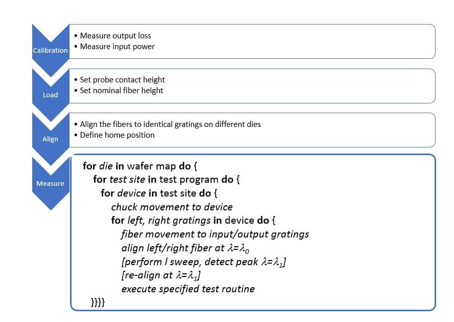
Finally, after wafer loading, optical calibration, and fiber alignment, the test program can be executed. This test program is different for each product, depending on the photonics components integrated in its design. To facilitate the testing, imec has developed a library of test routines, including loss measurement, detector measurement, modulator measurement, and scattering (S) parameter measurements.
Verifying reproducibility of measurement results
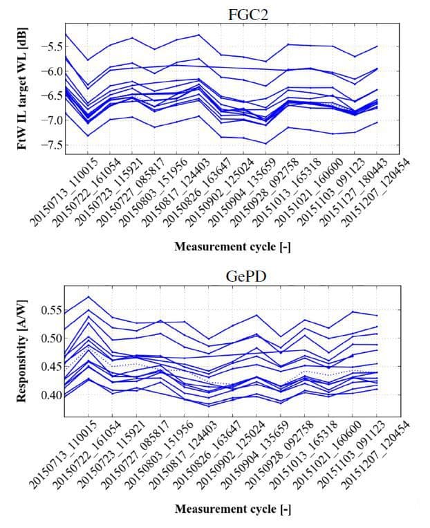
To ensure consistency among different data sets, the team has actively monitored the short-term repeatability and long-term reproducibility of the measurement data. To do so, they used a dedicated reference wafer. On this wafer, 14 dies were selected, each containing two different fiber-grating couplers (for transverse electric and transverse magnetic polarization of the incoming light) and one photodetector. These 14 dies are observed to give a statistically valid representation of the entire wafer. They are distributed uniformly over the entire wafer and are a mix of center and edge dies. The parameters of these dies (i.e., the fiber-to-wafer insertion loss and the detector responsivity) then were measured at regular time intervals. The repeatability/reproducibility is defined as the standard deviation of these data points for a given die.
Over a five-month period, a reproducibility of better than 0.8dB (±3 σ) in insertion loss was obtained, as was reproducibility of 0.09A/W in photodetector responsivity. Analysis of the measurement data revealed three main sources of variability: (1) a drift in the settings of the electronic polarization controller, (2) optical setup losses due to fibers being disconnected and reconnected, and (3) contamination of — or even damage to — the pigtail. These results stress the importance of performing periodic calibration and taking corrective action if needed.
From semi-automated optical tester to full-automatic configuration
The aforementioned electro-/optical testing system has been installed in imec’s optical test lab, and is in routine use for the wafer-level testing of Si photonics components. This test station is built around FormFactor’s Cascade PA300 semi-automatic ø300mm probe station and uses the electro/optical equipment setup and the positioning and alignment solutions developed by imec.
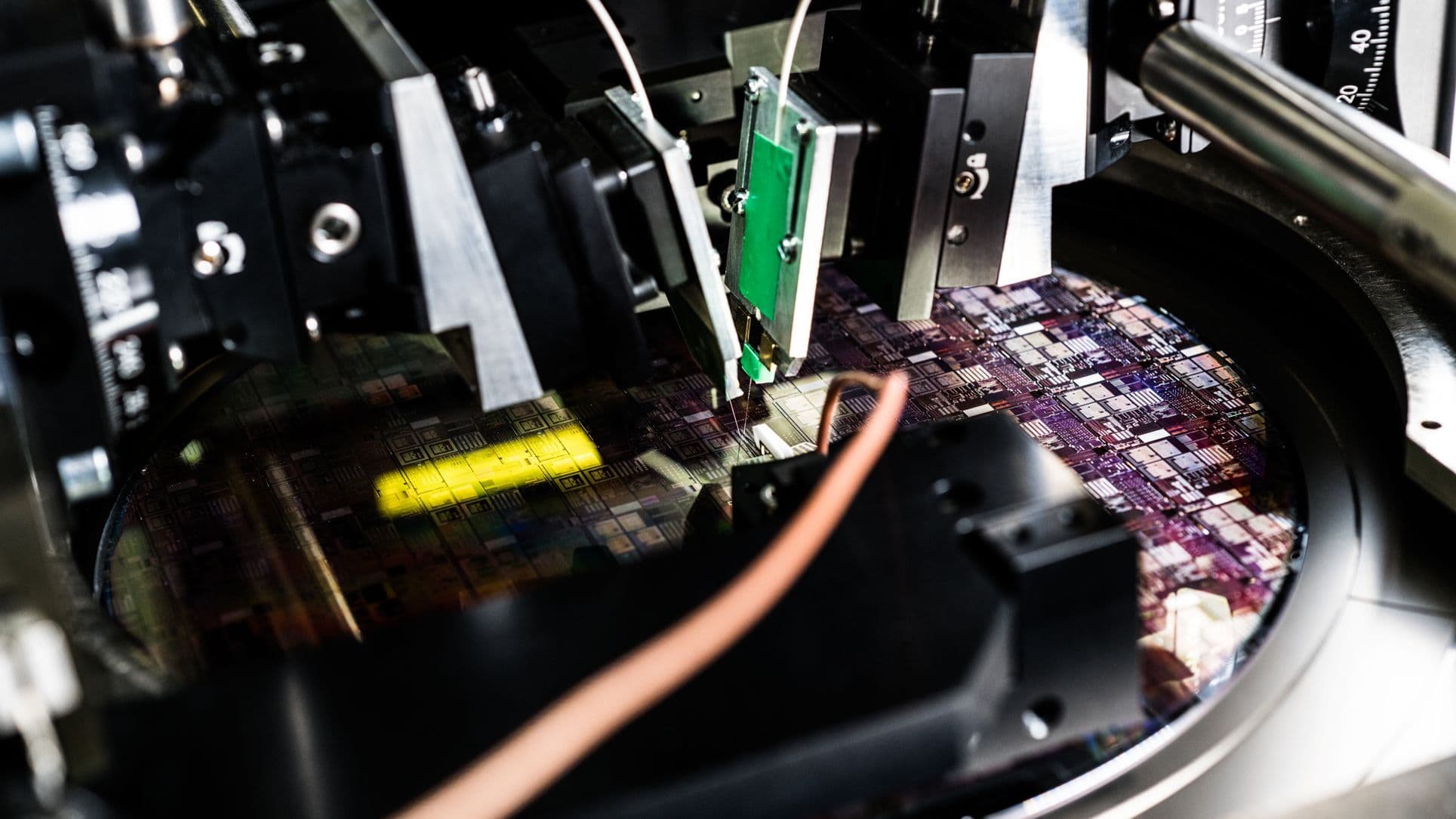
Moving forward, imec has selected FormFactor’s Cascade CM300xi as its next-generation probing platform for Si photonics development and manufacturing. This new wafer probe station includes an automated fiber positioning and piezo-based optical alignment solution, plus an automatic wafer loader, leading to a fully automatic configuration.
An additional route towards faster measurement times is the use of fiber arrays instead of single fibers. These fiber arrays can be considered as the optical equivalent of the electrical probe card, able to measure and test multiple optical devices in parallel.
Imec is exploring the use of Si V-groove assemblies containing up to 16 fibers. However, the optical calibration of a setup with fiber arrays is relatively complex, and requires dedicated calibration procedures that compensate for various error sources in the optical measurement system (e.g., coming from the variability within the fiber array itself, possible power splitters on- or off-chip, or different power meter channels).
Authors

Jeroen De Coster
Jeroen De Coster holds a master’s degree in Electrical Power Engineering (2001) and a PhD in Electrical Engineering (2006), both from KU Leuven. De Coster’s PhD work focused on the design, modelling and characterisation of RF-MEMS devices. Since 2006 he has worked for imec in Leuven, where he is developing measurement tools and procedures for functional characterization, as well as yield and reliability testing of MEMS, silicon photonics, and memory devices.

Erik Jan Marinissen
Erik Jan Marinissen is Principal Scientist at imec, where he is responsible for research on test and design-for-test. In addition, he is Visiting Researcher at Eindhoven University of Technology, the Netherlands. Previously, he worked at NXP Semiconductors and Philips Research Laboratories in Eindhoven. Marinissen holds an MSc degree in Computing Science (1990) and a PDEng degree in Software Technology (1992), both from Eindhoven University of Technology. He is (co-)author of 280+ journal and conference papers and (co-)inventor on 15 granted US/EP patent families. Marinissen is IEEE Fellow and Golden Core member of Computer Society.

Joris Van Campenhout
Joris Van Campenhout is Director of the Optical I/O industry-affiliation R&D program at imec, which targets the development of a scalable and industrially viable short-reach optical interconnect technology based on silicon photonics. Prior to joining imec in 2010, he was a post-doctoral researcher at IBM’s TJ Watson Research Center (USA). He obtained a PhD degree in Electrical Engineering from Ghent University (Belgium) in 2007, for his work on hybrid integration of electrically driven III-V microdisk lasers on silicon photonic waveguide circuits. Joris holds 7 patents and has authored or co-authored over 100 papers in the field of silicon integrated photonics.

Bryan C. Bolt
Bryan C. Bolt is Director of Engineering, Systems BU, at FormFactor, Inc. He has worked in the fields of optics and semiconductor capital equipment since 1988 in various engineering and technical management roles with companies including Etec Systems, Applied Materials, ESI, and Novellus Systems. Bryan holds a PhD in Electrical Engineering from the University of North Carolina at Charlotte and is a licensed Professional Mechanical Engineer (P.E.) in the state of Oregon.

Dan Rishavy
Dan Rishavy is a Director of Market Development for FormFactor’s systems business unit. Dan holds a degree in Electrical Engineering from the University of South Florida and an MBA from West Texas A&M University. He has been working in various aspects of the Semiconductor Test industry for over 20 years. Dan has held variety of roles in applications, product management and marketing throughout his career at Hewlett Packard, Agilent, Verigy, Tokyo Electron, Cascade Microtech, and FormFactor.
Discover more



Imec and Diraq demonstrate first coherent operation of eight silicon MOS spin qubits fabricated in a 300mm CMOS-compatible foundry process
Read more


Neural telemetry breakthrough: new chip delivers ten-fold compression while preserving signal integrity
Read more

