A 300mm platform for 2D-material based MOSFET devices
Unlocking 2D-material based FETs for high-performance logic applications: obstacles and paths.
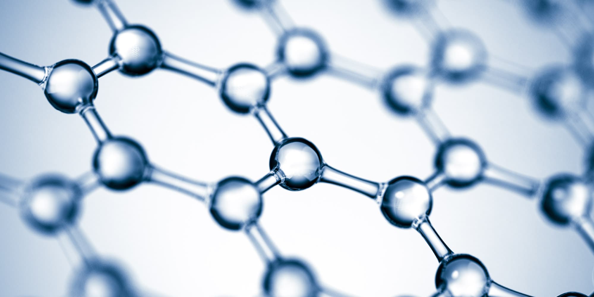
2D materials, a family of materials that form two-dimensional crystals, promise to enable a broad range of semiconductor applications, such as selectors or back-end compatible transistors. Integrated in the conduction channel of MOSFET devices, they may as well be used to create the ultimately scaled high-performance transistor. In this article, Iuliana Radu, beyond CMOS program director at imec, and her team discuss obstacles and paths towards designing 2D-based devices, integrating them in a 300mm platform, and optimizing their performance.
2D materials may enable multiple applications
In recent years, 2D crystals like graphene and transition metal dichalcogenides (MX2) have received considerable attention. The exceptional interest in these materials can be attributed to their remarkable properties. 2D crystals provide very interesting form-factors compared to traditional 3D crystals. In their elegant 2D form, electronic structure, mechanical flexibility, defect formation, and electronic and optical sensitivity become dramatically different.
The most known 2D material is graphene, a crystalline monolayer of carbon atoms arranged in a hexagonal honeycomb lattice structure. Graphene is flexible, transparent, and extremely strong. And it is a great thermal and electronic conductor. But the exploration of 2D materials has moved far beyond graphene. The class of MX2, for example, has versatile properties that complement those of graphene. E.g., they have a wide range of bandgaps as opposed to graphene, where the bandgap is absent. Interest in 2D materials reaches beyond semiconducting materials and includes the exploration of insulators and metals as well.
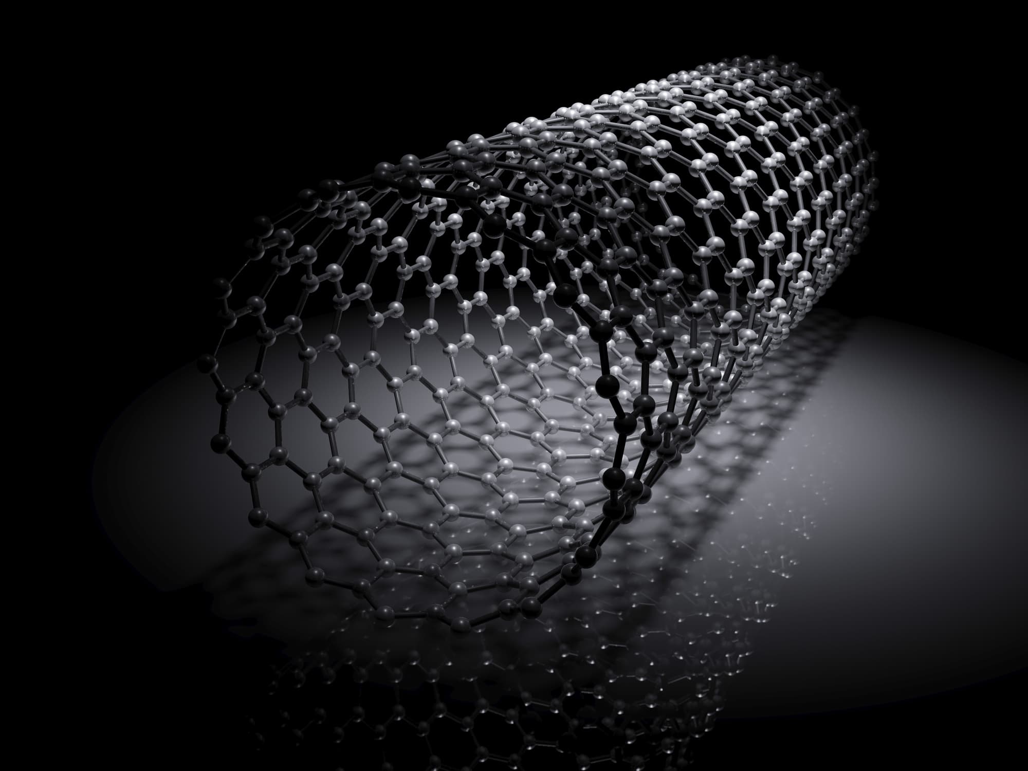
Opportunities for these materials have emerged in multiple domains, including (bio)sensing, energy storage, photovoltaics, opto-electronics and transistor scaling. Graphene, for example, is an ideal material for optoelectronics applications. It exhibits both electro-absorption and electro-refraction, making it suitable for light modulation, detection and switching. Recent investigations have demonstrated the potential of graphene-based integrated photonics for enabling the next-generation data- and telecom applications.
The new silicon?
Some of the 2D materials may even replace ‘good old’ Si in the channel of MOSFET devices. With Si in the conduction channel, gate length scaling induces short channel effects which degrade transistor performance. Replacing Si with 2D materials promises to counter the negative short-channel effects. Being atomically precise, the conduction channel can also be made very thin, down to the level of single atoms. In addition, several 2D materials have low dielectric constants that are comparable with Si oxide. This opens opportunities for building stacks with various 2D materials that have different functionalities (i.e., conduction channel, dielectric), and will enable gate length scaling down to a few nanometers. This way, 2D materials could provide an evolutionary path towards extreme device dimension scaling – targeting 3nm and below technology generations.
However, first implementation of 2D materials in electronic circuits will probably not be in ultimately scaled devices, but in low-power circuits that have less performance requirements (i.e., lower on-current). Examples include transistors and small circuits that can be implemented in the chips’ back-end-of-line. Here, they can relieve some of the routing congestion and save some area in the front-end-of-line. To build back-end compatible transistors, various materials are currently being investigated, including the semiconducting indium gallium zinc oxide (IGZO) and a variety of 2D materials.
A specific advantage of using 2D materials is the ability to build complementary MOS devices – i.e., nMOS and pMOS. And this allows the development of compact back-end logic circuits such as repeaters. A common requirement for these back-end transistors and circuits is the temperature budget, that should be compatible with back-end-of-line processing. 2D materials may also be used to build other circuits, such as on-chip power management systems, signal buffers and scalable memory selectors. For all these circuits, the current requirements (in terms of Ion) are relatively low, and – in contrast to highly scaled devices – one layer of 2D material will probably be sufficient to make the devices.
Towards a 300mm platform for 2D-material based devices
For ultimately scaled devices as well as for less demanding circuits, imec tries to understand the materials and process limitations of the 2D materials. More specifically, imec focuses on materials exploration (including 2D semiconductors, 2D (semi-)metals and 2D dielectrics), process integration exploration and device exploration. The team is setting up a generic integration flow that takes into account the common requirements for all applications, such as the allowed temperature budget and the chemical stability of the 2D materials. The integration flow targets 300mm wafers in order to leverage the benefits of high-volume manufacturing techniques. One important challenge is to maintain the single-crystal flake-like quality of the 2D materials during the 300mm integration process.
Unlocking 2D-material based FETs for high-performance logic
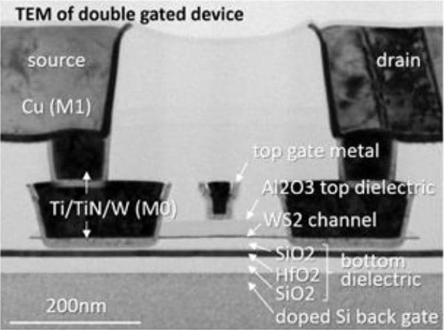
A double-gated WS2 FET architecture
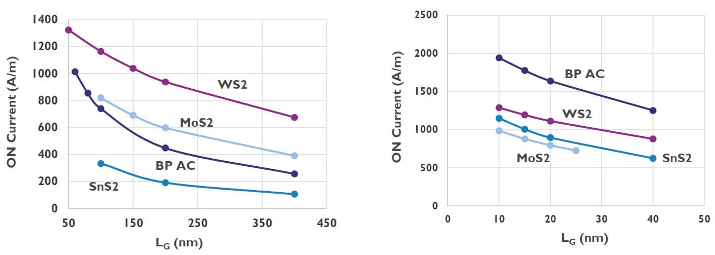
The development of ultimately scaled, high-performance devices starts with identifying the most promising 2D material and device architecture. Imec has therefore benchmarked different 2D materials and 2D FET architectures against an advanced Si FinFET platform.
From these studies, the imec team concluded that tungsten-disulfide (WS2) in a stacked nanosheet configuration has the highest performance potential (i.e., the highest on-current) amongst the 300mm technology compatible materials. They also concluded that a double-gated FET architecture is preferred over a single-gated FET, especially when the device structure suffers from non-idealities related to the contacts and spacer region.
Growth on 300mm wafers and subsequent layer transfer: a world’s first
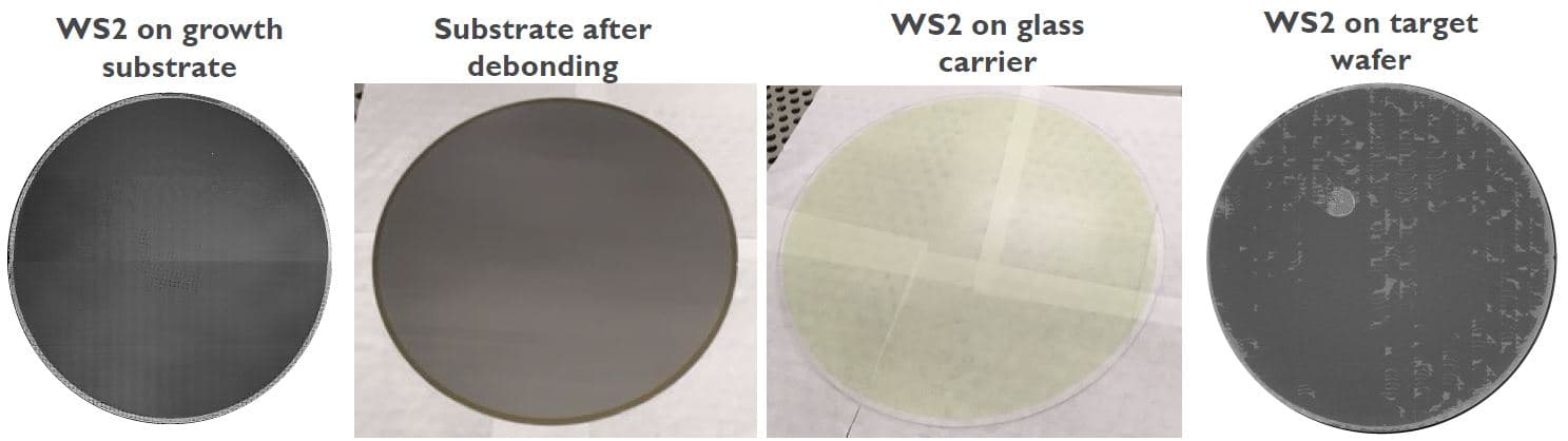
As a key process step in the device fabrication, high-quality growth of WS2 on 300mm wafers has been demonstrated for the first time using a modified metal-organic chemical vapor deposition (MOCVD) tool at imec. The approach results in thickness control with monolayer precision over the full 300mm wafer. The benefits of the MOCVD growth come however at the price of a high temperature when growing the material. To build a device integration flow which is compatible with back-end-of-line requirements, the subsequent transfer of the channel material from a growth substrate to a target device wafer is therefore crucial.
The imec team has developed a unique transfer process which allows the WS2 monolayer – as thin as 7 Ångstrom – to be successfully transferred to a target wafer. The transfer process is based on temporary bonding and debonding technologies, and has no impact on the electrical properties of the 2D material.
The technique has even been successfully applied on target substrates that have a certain topography. Future developments will focus on improving the transfer process even further in order to mitigate defects such as unwanted particles, markings on the front side and edge chipping.
Device challenges
On the device side, major challenges related to the gate dielectric, the metal contacts and the channel material defectivity and storage have been identified.
First, depositing dielectric materials on top of the 2D surface is a true challenge, due to the lack of dangling bonds on the (van der Waals terminated) 2D materials. The imec team is currently exploring two routes for dielectric growth: (1) direct atomic layer deposition (ALD) growth at reduced growth temperature, and (2) enhanced ALD nucleation by using a very thin oxidized layer (e.g. oxidized Si) as a nucleation layer. With the latter technique, preliminary measurements on a dual-gated configuration indicate a good capacitance with scaled dielectrics, both at the front and the back of the 2D material.
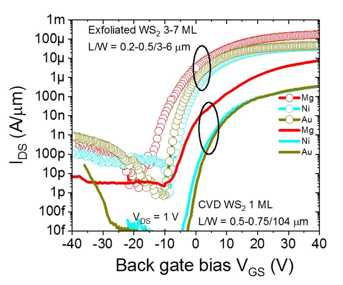
The imec team also screened a variety of metals to contact the WS2 nanosheet. They found that the highest on-current was obtained when using a Mg contact.
And finally, defects play a crucial role in the chemical behavior of the 2D materials, and hence profoundly impact the performance of the device. It is therefore crucial to understand the fundamentals of defect formation and the impact they have on device performance.
One of the most common defects in the channel material is sulfur vacancy. Imec is currently investigating how different plasma treatments can be used to passivate these defects. Besides, the materials’ stability and reactivity should be taken into account. 2D materials such as WS2 are known to quickly age and degrade. According to the team’s results, a promising approach against ageing is storing the samples in an inert environment.
Device performance: benchmark and outlook
Finally, the team has estimated the upper limits of the device performance, and what roads they should follow to get there.
As a benchmark, the imec team used dual-gated devices that were built with small, natural exfoliated WS2 flakes. For these lab-scale devices, mobility values >100cm2/Vs could be measured, which is close to the theoretically predicted mobility value for WS2. The expectation is that if this can be done with natural material, it should also be possible to get there with synthesized materials – which currently reach about a few cm2/Vs. Imec is working on improving the basic process steps which are expected to give a further performance increase.
For some of the main challenges ahead, the team has a clear view on how to solve them. For example, they know how to grow and transfer the material on a 300mm target substrate, and there is a clear integration road. They are also learning how to scale the gate dielectric, and how to improve the intrinsic mobility in the channel.
But down the integration paths, several challenges remain that require further investigation and better fundamental understanding. One of them is related to the poor adhesion of the 2D materials to the device wafer, another is the control of the threshold voltage. Solving these challenges will enable many of the electronic applications that are envisioned for 2D materials – ultimately scaled high-performance devices, as well as applications with less demanding specifications.
This work is the result of the collaborative effort of the imec exploratory device team and the imec nano applications materials engineering team.
Want to know more?
- ‘Imec reports for the first time direct growth of 2D materials on 300mm wafers’, press release
- Part of these results have been published in the 2018 IEDM paper ‘2D materials: roadmap to CMOS integration’ by C. Huyghebaert et al. This paper can be requested via this link.
- Part of this research is performed in the framework of the Graphene Flagship, a European Future and Emerging Technology Flagship initiative set up to take graphene and related layered materials from academic laboratories to everyday use. Read the imec magazine article on the Graphene Flagship, or visit the Graphene Flagship website.
Authors

Iuliana Radu
Iuliana Radu is program director at imec, where she is leading the beyond CMOS and quantum computing activities. Prior to joining the logic program at imec in 2013, she was a Marie Curie and FWO fellow at KU Leuven and imec. Her work at imec and KU Leuven includes devices using the metal-to-insulator transition, ionic and electronic transport in functional oxides and devices with graphene and other 2D materials. Iuliana has received a PhD in physics from MIT in 2009 where she worked on the fractional quantum Hall effect and searched for non-abelian quasiparticles.
Discover more



Imec and Diraq demonstrate first coherent operation of eight silicon MOS spin qubits fabricated in a 300mm CMOS-compatible foundry process
Read more


Neural telemetry breakthrough: new chip delivers ten-fold compression while preserving signal integrity
Read more

