Imec reports for the first time direct growth of 2D materials on 300mm wafers
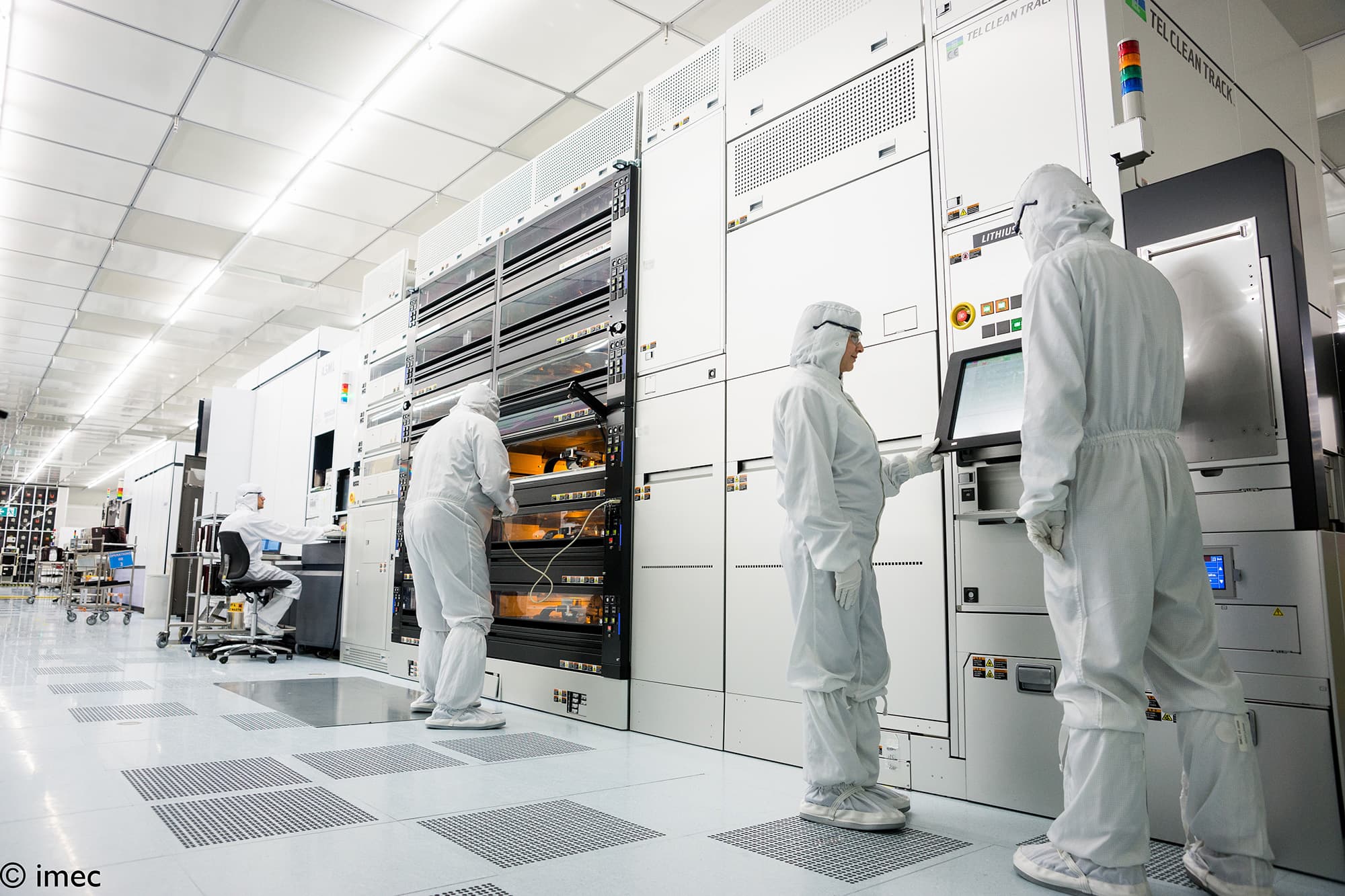
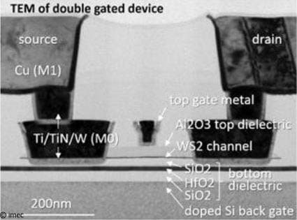
SAN FRANCISCO (USA), DECEMBER 3, 2018 — This week, at the 2018 IEEE International Electron Devices Meeting (IEDM), imec, the world-leading research and innovation hub in nanoelectronics and digital technologies, presents a 300mm-wafer platform for MOSFET devices with 2D materials. 2D materials could provide the path towards extreme device-dimension scaling as they are atomically precise and suffer little from short channel effects. Other possible applications of 2D materials could come from using them as switches in the BEOL, which puts an upper limit on the allowed temperature budget in the integration flow.
The imec platform integrates as transistor channel WS2, a 2D material which holds promise for higher ON current compared to most other 2D materials and good chemical stability. Imec reports here for the first time the MOCVD growth of WS2 on 300mm wafers, a key process step for device fabrication. The MOCVD synthesis approach results in thickness control with monolayer precision over the full 300mm wafer and potentially highest mobility material. The benefits of the MOCVD growth come at the price of a high temperature while growing the material.
To build a device integration flow which could be compatible with BEOL requirements, the transfer of the channel material from a growth substrate to a device wafer is crucial. Imec is the first to demonstrate a full 300mm monolayer 2D material transfer, which is very challenging on its own because of the low adhesion of 2D materials to the device wafer and to the exteme thinness of the material transferred: 0.7nm! The transfer process was developed together with SUSS MicroTec and Brewer Science using temporary bonding and debonding technologies. WS2 wafers are temporarily bonded to glass carrier wafers using a specially formulated material (Brewer Science). Next, the WS2 monolayer is mechanically debonded from the growth wafer and bonded again in vacuum to the device wafer. The carrier wafer is removed using laser debonding. This debonding technique is a key enabler for the controlled transfer of 2D materials
Iuliana Radu, Beyond CMOS Program Director at imec, explains, “Building the 300mm platform for MOSFET device study with 2D materials and developing the process step ecosystem speeds-up the technological adoption of these materials. Several challenges are still to be resolved and are the subject of ongoing research and development.” Major challenges include scaling the equivalent oxide thickness (EOT) of gate dielectric for 2D materials, and reducing channel defectivity to boost mobility.
Imec’s research into advanced logic scaling is performed in cooperation with imec’s key CMOS program partners including GlobalFoundries, Huawei, Intel, Micron, Qualcomm, Samsung, SK Hynix, Sony Semiconductor Solutions, TOSHIBA Memory, TSMC and Western Digital.
About imec
Imec is the world-leading research and innovation hub in nanoelectronics and digital technologies. The combination of our widely acclaimed leadership in microchip technology and profound software and ICT expertise is what makes us unique. By leveraging our world-class infrastructure and local and global ecosystem of partners across a multitude of industries, we create groundbreaking innovation in application domains such as healthcare, smart cities and mobility, logistics and manufacturing, energy and education.
As a trusted partner for companies, start-ups and universities we bring together more than 4,000 brilliant minds from over 85 nationalities. Imec is headquartered in Leuven, Belgium and has distributed R&D groups at a number of Flemish universities, in the Netherlands, Taiwan, USA, China, and offices in India and Japan. In 2017, imec's revenue (P&L) totaled 546 million euro. Further information on imec can be found at www.imec-int.com.
Imec is a registered trademark for the activities of IMEC International (a legal entity set up under Belgian law as a "stichting van openbaar nut”), imec Belgium (IMEC vzw supported by the Flemish Government), imec the Netherlands (Stichting IMEC Nederland, part of Holst Centre which is supported by the Dutch Government), imec Taiwan (IMEC Taiwan Co.) and imec China (IMEC Microelectronics (Shanghai) Co. Ltd.) and imec India (Imec India Private Limited), imec Florida (IMEC USA nanoelectronics design center).
Discover more



Imec and Diraq demonstrate first coherent operation of eight silicon MOS spin qubits fabricated in a 300mm CMOS-compatible foundry process
Read more


Neural telemetry breakthrough: new chip delivers ten-fold compression while preserving signal integrity
Read more

