Sequential Infiltration Synthesis (SIS) significantly improves EUV patterning
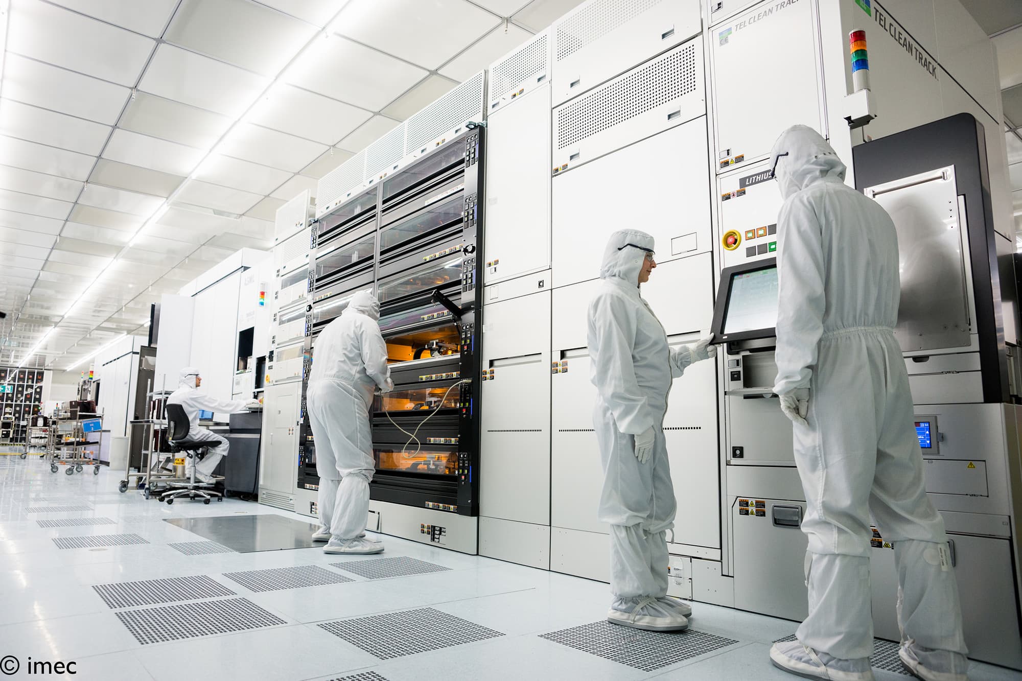
SAN FRANCISCO (US), FEBRUARY 25, 2019 — This week, at the SPIE Advanced Lithography conference 2019, imec, a world-leading research and innovation hub in nanoelectronics and digital technologies, demonstrates the positive impact of sequential infiltration synthesis (SIS) on the EUVL (extreme ultra-violet lithography) patterning process. This post-lithography technique is shown to significantly reduce stochastic nano-failures and line roughness, contributing to the introduction of EUVL patterning of future nodes”. This work integrates recent advancements on metrology and etch, and on material developments, which will be presented in multiple papers at this week’s 2019 SPIE Advanced Lithography Conference.
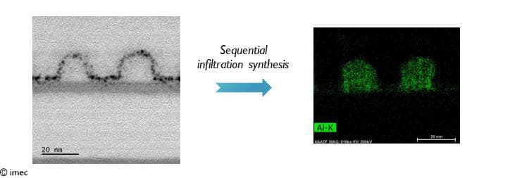
SIS is an existing technique, used in directed self-assembly (DSA) and now applied in EUV lithography, in which the photoresist is infiltrated with an inorganic element to make it harder and more robust, thereby enhancing the patterning performance on different parameters. Imec and partners show the first comparison between an EUVL-SIS and a standard EUVL patterning process demonstrating the benefits of SIS regarding roughness, nano-failure mitigation and local variability. When adding an SIS step during a full pattern transfer in a TiN layer, imec observed a improvement of 60 % for intrafield local critical dimension uniformity (LCDU) and 10% for line edge roughness compared to a reference process. These patterning enhancements are inherent properties of SIS. Also, the number of nanobreaks – a typical stochastic nano-failure – is reduced by at least one order of magnitude. Results were confirmed in an industrial relevant use case, showing reduced defectivity in a logic chip with a 20% smaller tip-to-tip critical dimension at a similar LCDU as a standard EUVL process.
The improvement SIS showcases on all parameters is indebted to imec’s EUV lithography and metrology infrastructure and recent advancements in the field of process control, material and etch research. The current work brings these results and competences together in one paper, establishing SIS as a significant EUV patterning enhancement technique. The progress on each of the integrated aspects and SIS will be presented on the SPIE Advanced Lithography conference in multiple papers.
The work was performed in collaboration with ASM and ASML.
"The recent achievements with SIS for EUV lithography were enabled by the progress imec and its partners have made in various domains such as materials science, deposition, imaging, and metrology. This is a great example of how the integration of knowledge and combined efforts from multiple domains and ecosystem partners will enable a path to scale to N3 and beyond." Greg McIntyre, director of advanced patterning at imec.
About imec
Imec is a world-leading research and innovation hub in nanoelectronics and digital technologies. The combination of our widely acclaimed leadership in microchip technology and profound software and ICT expertise is what makes us unique. By leveraging our world-class infrastructure and local and global ecosystem of partners across a multitude of industries, we create groundbreaking innovation in application domains such as healthcare, smart cities and mobility, logistics and manufacturing, energy and education.
As a trusted partner for companies, start-ups and universities we bring together more than 4,000 brilliant minds from over 85 nationalities. Imec is headquartered in Leuven, Belgium and has distributed R&D groups at a number of Flemish universities, in the Netherlands, Taiwan, USA, China, and offices in India and Japan. In 2017, imec's revenue (P&L) totaled 546 million euro. Further information on imec can be found at www.imec-int.com.
Imec is a registered trademark for the activities of IMEC International (a legal entity set up under Belgian law as a "stichting van openbaar nut”), imec Belgium (IMEC vzw supported by the Flemish Government), imec the Netherlands (Stichting IMEC Nederland, part of Holst Centre which is supported by the Dutch Government), imec Taiwan (IMEC Taiwan Co.) and imec China (IMEC Microelectronics (Shanghai) Co. Ltd.) and imec India (Imec India Private Limited), imec Florida (IMEC USA nanoelectronics design center).
Discover more



Imec and Diraq demonstrate first coherent operation of eight silicon MOS spin qubits fabricated in a 300mm CMOS-compatible foundry process
Read more


Neural telemetry breakthrough: new chip delivers ten-fold compression while preserving signal integrity
Read more

