Imec’s high-speed ultrasonic SNAPSCAN camera enables hyperspectral imaging acquisition in less than one second

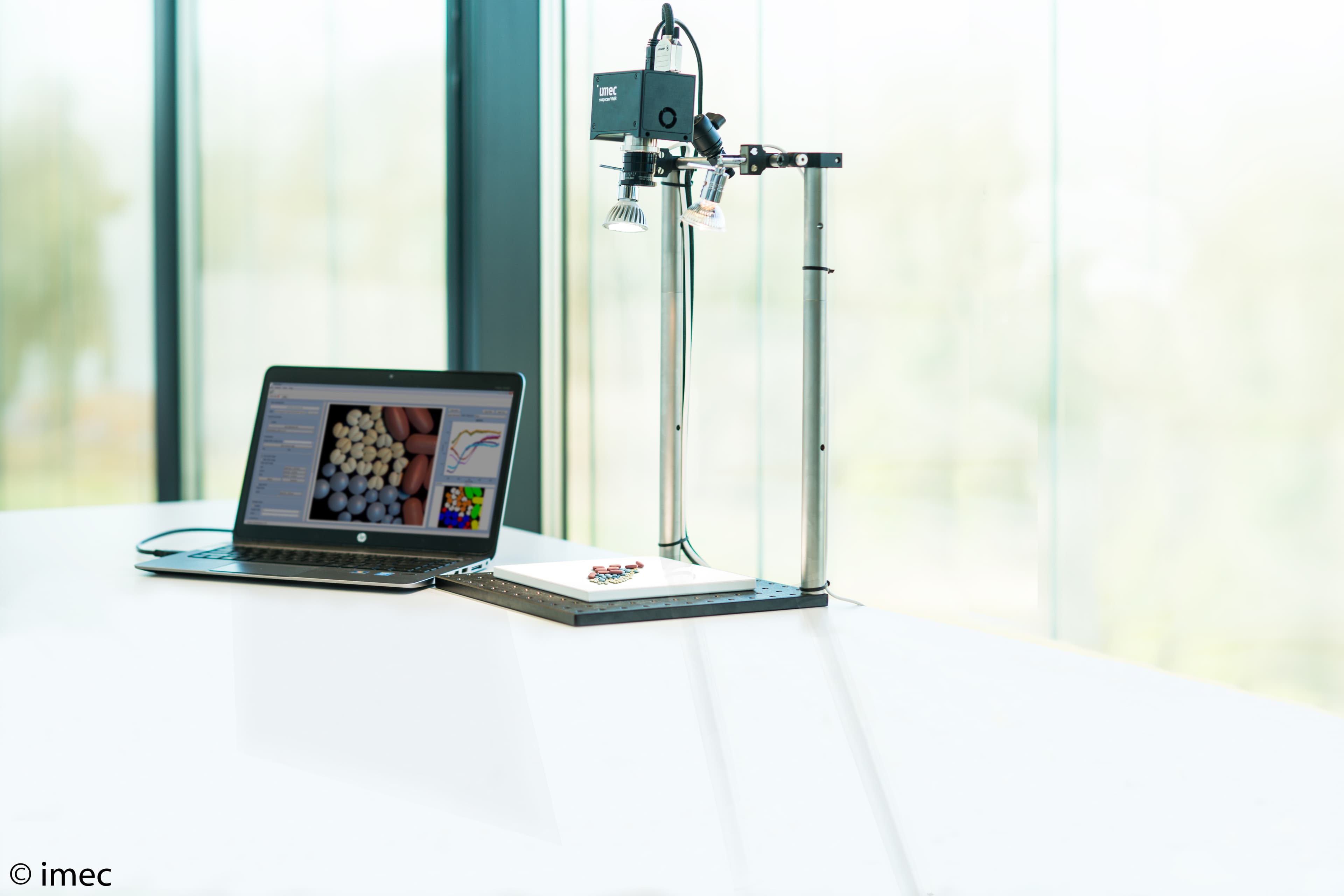
SAN FRANCISCO — Jan. 29, 2018 – Imec, the world-leading research and innovation hub in nanoelectronics and digital technologies, today announced that it will demonstrate at this week’s SPIE Photonics West in San Francisco its second generation high-speed SNAPSCAN hyperspectral imaging camera. The new hyperspectral camera uses an ultrasonic speed piezo motor stage and innovative software to enable the acquisition of high resolution hyperspectral images in less than 200ms. It will enable our partners to develop consistent spectral libraries and customized solutions faster than ever possible before, and this for a wide range of new applications in the medical market.
The SNAPSCAN hyperspectral camera is a proprietary breakthrough system concept initially introduced by imec one year ago. It combines a high signal-to-noise ratio and high spatial and spectral resolutions with the user friendliness of a snapshot hyperspectral imaging camera.
“We have been thrilled by the commercial success of the first generation SNAPSCAN camera which was introduced at SPIE Photonics West 2017,” explained Andy Lambrechts, program manager for integrated imaging activities at imec. “By introducing an ultrasonic speed piezo motor stage, we can now guarantee image acquisition times of less than a second, and thus minimize the effects of motion artifacts during acquisition. As a result, we can now enable many more key applications such as digital pathology, wound healing, skin diagnostics and guided surgery.”
Imec’s new SNAPSCAN camera handles all scanning internally using the miniaturized ultrasonic piezo scanning stage, thereby excluding the need for external scanning movement. Today, spatial resolution of 3,650 x 2,048px (7MPx), with a spectral resolution of 150+ spectral bands can be reached over the VNIR spectral range (470 – 900nm) and the NIR range (600 – 975nm). With imec’s proprietary hyperspectral imaging acquisition software, specific spectral regions of interest can now be selected, which enables acquiring images at a very high speed of only 200ms. Flat signal-to-noise ratios of 200:1 over the full spectral range are in reach, with optimized acquisition and lighting set-up parameters.
“We believe our new high-speed ultrasonic SNAPSCAN camera technology will further open the market for all users who intend to bridge the gap between academic research and commercial development. The second generation ultrasonic high-speed SNAPSCAN camera ability to easily create high quality datasets will enable our partners to move from initial application validation to building consistent spectral libraries and application solutions faster than ever possible before,” explains Jerome Baron, business development manager at imec’s integrated imaging and vision system teams. “With a full year of commercialization under our belts, we have validated many clear commercial opportunities beyond the R&D market such as the medical market.”
Imec’s ultrasonic SNAPSCAN hyperspectral imaging cameras are demonstrated for the first time at SPIE Photonic West, booth #4321 in the North Hall of the Moscone center in San-Francisco and will be commercially available in April 2018.
About imec
Imec is the world-leading research and innovation hub in nanoelectronics and digital technologies. The combination of our widely acclaimed leadership in microchip technology and profound software and ICT expertise is what makes us unique. By leveraging our world-class infrastructure and local and global ecosystem of partners across a multitude of industries, we create groundbreaking innovation in application domains such as healthcare, smart cities and mobility, logistics and manufacturing, energy and education.
As a trusted partner for companies, start-ups and universities we bring together close to 3,500 brilliant minds from over 70 nationalities. Imec is headquartered in Leuven, Belgium and has distributed R&D groups at a number of Flemish universities, in the Netherlands, Taiwan, USA, China, and offices in India and Japan. In 2016, imec's revenue (P&L) totaled 496 million euro. Further information on imec can be found at www.imec-int.com.
Imec is a registered trademark for the activities of IMEC International (a legal entity set up under Belgian law as a "stichting van openbaar nut”), imec Belgium (IMEC vzw supported by the Flemish Government), imec the Netherlands (Stichting IMEC Nederland, part of Holst Centre which is supported by the Dutch Government), imec Taiwan (IMEC Taiwan Co.) and imec China (IMEC Microelectronics (Shanghai) Co. Ltd.) and imec India (Imec India Private Limited), imec Florida (IMEC USA nanoelectronics design center).
Contact
Hanne Degans, Press communications manager, +32 16 28 17 69 // +32 486 06 51 75 // Hanne.Degans@imec.be
Discover more



Imec and Diraq demonstrate first coherent operation of eight silicon MOS spin qubits fabricated in a 300mm CMOS-compatible foundry process
Read more


Neural telemetry breakthrough: new chip delivers ten-fold compression while preserving signal integrity
Read more

