Imec Reports Breakthrough in Extending Interconnects Beyond the 3nm Technology Node

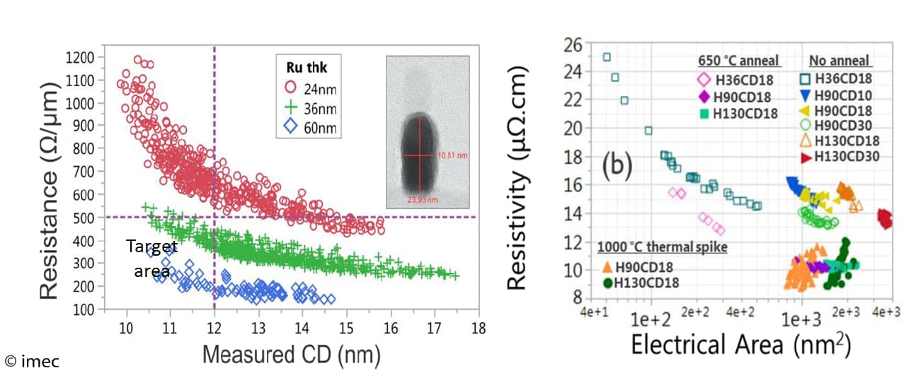
LEUVEN (Belgium), July 9, 2018 — Today at its annual Imec Technology Forum USA in San Francisco, imec, the world-leading research and innovation hub in nanoelectronics and digital technology, imec reports on the potential of using ruthenium (Ru) as a disruptive interconnect material for 3nm and beyond technology nodes. High-aspect ratio Ru lines were shown to outperform conventional Cu metallization in two different implementation scenarios, i.e., (1) in buried power rail applications, and (2) as interconnects for advanced memory and logic applications by using subtractive metal etch.
Due to an increasing resistance-capacitance delay and rising reliability concerns, the use of dual-damascene Cu as a process flow for back-end-of-line interconnect fabrication has become questionable beyond the 5nm technology node. To maintain the scaling paths, imec has therefore been pioneering and pipelining the potential replacement of this conventional Cu technology. Interconnects based on Ru are a promising candidate, because of their resistance to oxidation, high melting point, low bulk resistivity, and the ability to build barrier-less interconnect modules. Zsolt Tokei, Distinghuished Member of the Technical Staff at imec:
“For more than five years, imec has been systematically investigated this disruptive alternative, from the fundamentals to module level implementation. The results have recently come to the point of strong industrial interest.”
Imec used Ru-based interconnects in two different implementation scenarios. In a first application, Ru lines with aspect ratio (AR) up to 7 and critical dimension (CD) of 18nm were applied as a power rail, buried in the chip’s front-end-of-line oxide isolation. Traditionally, power rails are implemented as Cu lines in the metal-1 layer. The use of buried power rails has however recently emerged as a scaling booster, helping to minimize the standard cell height. Imec’s high-AR Ru lines, fabricated using a spacer defined integration scheme, exhibit low line resistivity of 8.8µΩcm, high stability, and withstand high temperature budget. With these characteristics, they can successfully be used as a buried power rail in sub-5nm technology nodes.
In a second implementation scenario, imec applied subtractive etch of Ru films to fabricate high-aspect ratio back-end-of-line interconnects for sub-5nm technology nodes. Imec demonstrated 12nm working Ru lines with aspect ratio up to 3.8, and line resistance below 500Ω/µm, and demarcated the technology targets for the 3nm node. Zsolt Tokei: “Our work proves that subtractive metal etch – which was used in the past for integrating Al interconnects – can be a valid alternative to the damascene implementation of Ru. The integration scheme has a strong downscaling potential, and can be considered for advanced memory and logic applications.”
Furthermore, using Si data and modeling, calibrated line and via resistance models have been developed for Ru, allowing to predict the resistance behavior of Ru in future scenarios. Besides Ru, other pure metals, as well as graphene, binary and ternary compounds were found to potentially provide long-term material pipeline for interconnects.
About imec
Imec is the world-leading research and innovation hub in nanoelectronics and digital technologies. The combination of our widely acclaimed leadership in microchip technology and profound software and ICT expertise is what makes us unique. By leveraging our world-class infrastructure and local and global ecosystem of partners across a multitude of industries, we create groundbreaking innovation in application domains such as healthcare, smart cities and mobility, logistics and manufacturing, energy and education.
As a trusted partner for companies, start-ups and universities we bring together close to 4,000 brilliant minds from over 85 nationalities. Imec is headquartered in Leuven, Belgium and has distributed R&D groups at a number of Flemish universities, in the Netherlands, Taiwan, USA, China, and offices in India and Japan. In 2017, imec's revenue (P&L) totaled 546 million euro. Further information on imec can be found at www.imec-int.com.
Imec is a registered trademark for the activities of IMEC International (a legal entity set up under Belgian law as a "stichting van openbaar nut”), imec Belgium (IMEC vzw supported by the Flemish Government), imec the Netherlands (Stichting IMEC Nederland, part of Holst Centre which is supported by the Dutch Government), imec Taiwan (IMEC Taiwan Co.) and imec China (IMEC Microelectronics (Shanghai) Co. Ltd.) and imec India (Imec India Private Limited), imec Florida (IMEC USA nanoelectronics design center).
Contact
Hanne Degans, press communications manager, +32 16 28 17 69 // +32 486 06 51 75 // Hanne.Degans@imec.be
Discover more



Imec and Diraq demonstrate first coherent operation of eight silicon MOS spin qubits fabricated in a 300mm CMOS-compatible foundry process
Read more


Neural telemetry breakthrough: new chip delivers ten-fold compression while preserving signal integrity
Read more

