Imec Pushes the Limits of EUVL Single Exposure for Logic N5 Metal Layers and Dense DRAM Applications
Imec presents initial electrical results on N5 32nm pitch metal-2 layer

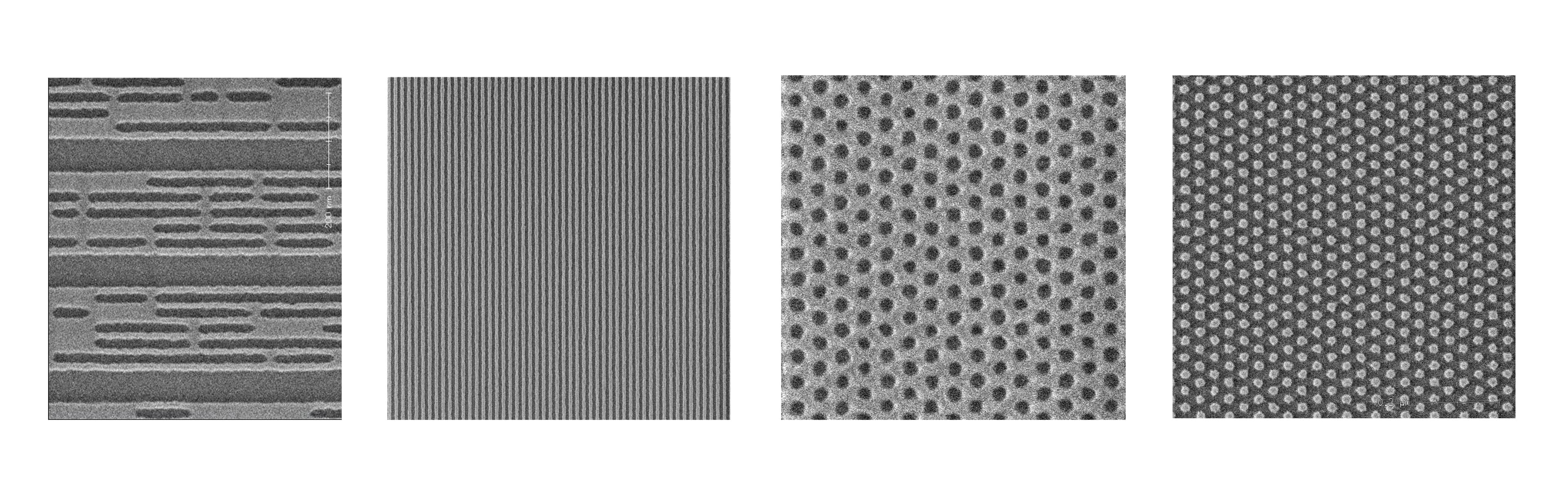
LEUVEN (Belgium), February 26, 2018 – Imec, the world-leading research and innovation hub in nanoelectronics and digital technology, continues to advance the readiness of EUV lithography (EUVL) with particular focus on EUV single exposure of Logic N5 metal layers, and of aggressive dense hole arrays. Imec’s approach to enable EUV single patterning at these dimensions is based on the co-optimization of various lithography enablers, including materials, metrology, design rules, post processing and a fundamental understanding of critical EUV processes. The results, that will be presented in multiple papers at this week’s 2018 SPIE Advanced Lithography Conference, are aimed at significantly impacting the technology roadmap and wafer cost of near-term technology nodes for logic and memory.
With the industry making significant improvements in EUV infrastructure readiness, first insertion of EUV lithography in high-volume manufacturing is expected in the critical back-end-of-line metal and via layers of the foundry N7 Logic technology node, with metal pitches in the range of 36–40nm. Imec’s research focuses on the next node (32nm pitch and below), where various patterning approaches are being considered. These approaches vary considerably in terms of complexity, wafer cost, and time to yield, and include variations of EUV multipatterning, hybrid EUV and immersion multipatterning, and EUV single expose. At SPIE last year, imec presented many advances in hybrid multipatterning and revealed various challenges of the more cost-effective EUV single exposure solution. This year, imec and its partners show considerable progress towards enabling these dimensions with EUV single exposure.
Imec’s path comprises a co-optimization of various lithography enablers, including resist materials, stack and post processing, metrology, computational litho and design-technology co-optimization, and a fundamental understanding of EUV resist reaction mechanisms and of stochastic effects. Based on this comprehensive approach, imec has demonstrated promising advances including initial electrical results, on EUV single exposure focusing on two primary use cases: logic N5 32nm pitch metal-2 layer and 36nm pitch contact hole arrays.
Working with its many materials partners, imec assessed different resist materials strategies, including chemically amplified resists, metal-containing resists and sensitizer-based resists. Particular attention was paid to the resist roughness, and to nano-failures such as nanobridges, broken lines or missing contacts that are induced by the stochastic EUV patterning regime. These stochastic failures are currently limiting the minimum dimensions for single expose EUV. Based on this work, imec delved into the fundemental understanding of stochastics and identified the primary dependencies influencing failures. Additionally, various metrology techniques and hybrid strategies have been employed to ensure an accurate picture of the reality of stochastics. Imec will report on this collective work, demonstrating the performance of various state-of-the-art line-space and contact hole resists.
As resist materials advances alone will likely be inssufient to meet the requirements, imec has also focused on co-optimizing the photomask, film stack, EUV exposures and etch towards an integrated patterning flow to achieve full patterning of the structures. This was done using computational lithography techniques such as optical proximity correction and source mask optimization, complemented by design-technology co-optimization to reduce standard library cell areas. Finally, etch-based post-processing techniques aimed at smoothing the images after the lithography steps yields encouraging results for dense features. Co-optimization of these multiple knobs is key to achieving optimized patterning and edge placement error control.
Greg McIntyre, Director of advanced patterning at imec summarizes:
“We feel these are very promising advances towards enabling EUV to reliably achieve single patterning at these aggressive dimensions. This would significantly impact the cost effectiveness of patterning solutions for the next few technology nodes.”
About imec
Imec is the world-leading research and innovation hub in nanoelectronics and digital technologies. The combination of our widely acclaimed leadership in microchip technology and profound software and ICT expertise is what makes us unique. By leveraging our world-class infrastructure and local and global ecosystem of partners across a multitude of industries, we create groundbreaking innovation in application domains such as healthcare, smart cities and mobility, logistics and manufacturing, energy and education.
As a trusted partner for companies, start-ups and universities we bring together close to 3,500 brilliant minds from over 70 nationalities. Imec is headquartered in Leuven, Belgium and has distributed R&D groups at a number of Flemish universities, in the Netherlands, Taiwan, USA, China, and offices in India and Japan. In 2016, imec's revenue (P&L) totaled 496 million euro. Further information on imec can be found at www.imec-int.com.
Imec is a registered trademark for the activities of IMEC International (a legal entity set up under Belgian law as a "stichting van openbaar nut”), imec Belgium (IMEC vzw supported by the Flemish Government), imec the Netherlands (Stichting IMEC Nederland, part of Holst Centre which is supported by the Dutch Government), imec Taiwan (IMEC Taiwan Co.) and imec China (IMEC Microelectronics (Shanghai) Co. Ltd.) and imec India (Imec India Private Limited), imec Florida (IMEC USA nanoelectronics design center).
Contact
Hanne Degans, press communications manager, +32 16 28 17 69 // +32 486 06 51 75 // Hanne.Degans@imec.be
Discover more



Imec and Diraq demonstrate first coherent operation of eight silicon MOS spin qubits fabricated in a 300mm CMOS-compatible foundry process
Read more


Neural telemetry breakthrough: new chip delivers ten-fold compression while preserving signal integrity
Read more

