Imec Extends Damascene Metallization Towards the 3nm Technology Node
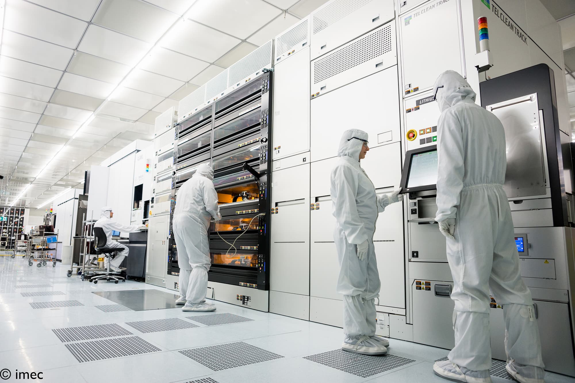
LEUVEN, June 4, 2018 – At this week’s 2018 IEEE International Interconnect Technology Conference (IITC 2018), imec, the world-leading research and innovation hub in nanoelectronics and digital technology, will present 11 papers on advanced interconnects, ranging from extending Cu and Co damascene metallization, all the way to evaluating new alternatives such as Ru and graphene. After careful evaluation of the resistance and reliability behavior, imec takes first steps towards extending conventional metallization into to the 3nm technology node.
For almost two decades, Cu-based dual damascene has been the workhorse industrial process flow for building reliable interconnects. But when downscaling logic device technology towards the 5nm and 3nm technology nodes, meeting resistance and reliability requirements for the tightly pitched Cu lines has become increasingly challenging. The industry is however in favor of extending the current damascene technology as long as possible, and therefore, different solutions have emerged.
To set the limits of scaling, imec has benchmarked the resistance of Cu with respect to Co and Ru in a damascene vehicle with scaled dimensions, demonstrating that Cu still outperforms Co for wire cross sections down to 300nm2 (or linewidths of 12nm), which corresponds to the 3nm technology node. To meet reliability requirements, one option is to use Cu in combination with thin diffusion barriers such as tantalum nitride (TaN)) and liners such as Co or Ru. It was found that the TaN diffusion barrier can be scaled to below 2nm while maintaining excellent Cu diffusion barrier properties.
For Cu linewidths down to 15–12nm, imec also modeled the impact of the interconnect line-edge roughness on the system-level performance. Line-edge roughness is caused by the lithographic and patterning steps of interconnect wires, resulting in small variations in wire width and spacing. At small pitches, these can affect the Cu interconnect resistance and variability. Although there is a significant impact of line-edge roughness on the resistance distribution for short Cu wires, the effect largely averages out at the system level.
An alternative solution to extend the traditional damascene flow is replacing Cu by Co. Today Co requires a diffusion barrier – an option that recently gained industrial acceptance. A next possible step is to enable barrierless Co or at least sub-nm barrier thickness with careful interface engineering. Co has the clear advantage of having a lower resistance for smaller wire cross-secions and smaller vias. Based on electromigration and thermal storage experiments, imec presents a detailed study of the mechanisms that impact Co via reliability, showing the abscence of voids in barrierless Co vias, demonstrating a better scalability of Co towards smaller nodes.
The research is performed in cooperation with imec’s key nano interconnect program partners including GlobalFoundries, Huawei, Intel, Micron, Qualcomm, Samsung, SK Hynix, SanDisk/Western Digital, Sony Semiconductor Solutions, TOSHIBA Memory and TSMC.
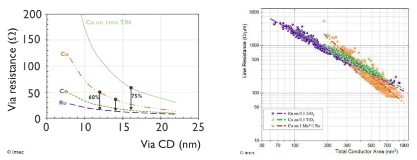
Via resistance for Co, Cu, Ru (left); and comparison of damascene line resistance versus total conductor cross-sections area of Ru, Co and Cu nanowires (right)
About imec
Imec is the world-leading research and innovation hub in nanoelectronics and digital technologies. The combination of our widely acclaimed leadership in microchip technology and profound software and ICT expertise is what makes us unique. By leveraging our world-class infrastructure and local and global ecosystem of partners across a multitude of industries, we create groundbreaking innovation in application domains such as healthcare, smart cities and mobility, logistics and manufacturing, energy and education.
As a trusted partner for companies, start-ups and universities we bring together close to 4,000 brilliant minds from over 85 nationalities. Imec is headquartered in Leuven, Belgium and has distributed R&D groups at a number of Flemish universities, in the Netherlands, Taiwan, USA, China, and offices in India and Japan. In 2017, imec's revenue (P&L) totaled 546 million euro. Further information on imec can be found at www.imec-int.com.
Imec is a registered trademark for the activities of IMEC International (a legal entity set up under Belgian law as a "stichting van openbaar nut”), imec Belgium (IMEC vzw supported by the Flemish Government), imec the Netherlands (Stichting IMEC Nederland, part of Holst Centre which is supported by the Dutch Government), imec Taiwan (IMEC Taiwan Co.) and imec China (IMEC Microelectronics (Shanghai) Co. Ltd.) and imec India (Imec India Private Limited), imec Florida (IMEC USA nanoelectronics design center).
Contact
Hanne Degans, press communications manager, +32 16 28 17 69 // +32 486 06 51 75 // Hanne.Degans@imec.be
Discover more



Imec and Diraq demonstrate first coherent operation of eight silicon MOS spin qubits fabricated in a 300mm CMOS-compatible foundry process
Read more


Neural telemetry breakthrough: new chip delivers ten-fold compression while preserving signal integrity
Read more

