Imec demonstrates manufacturability of state-of-the-art spin-orbit torque MRAM devices on 300mm Si wafers
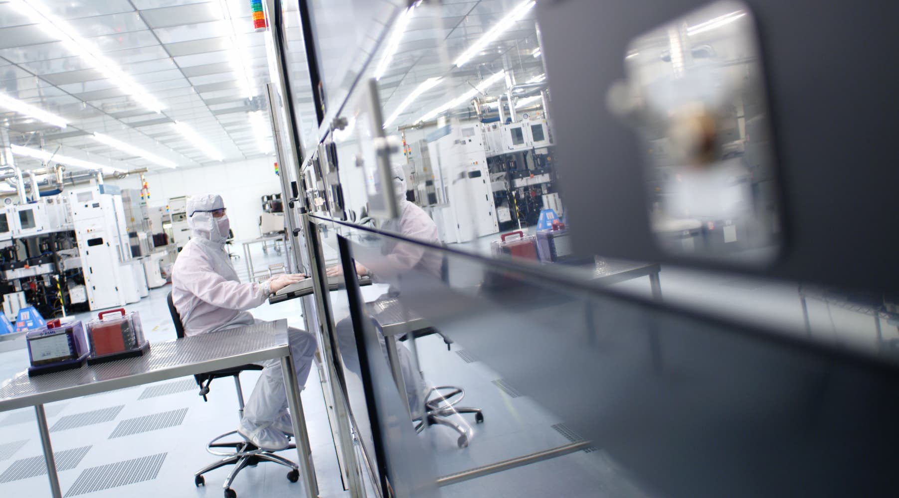
LEUVEN (Belgium), June 18, 2018 – At this week’s 2018 Symposia on VLSI Technology and Circuits, imec, the world-leading research and innovation hub in nanoelectronics and digital technology, demonstrates for the first time the possibility to fabricate state-of-the-art spin-orbit torque MRAM (SOT-MRAM) devices on 300mm wafers using CMOS compatible processes. With an unlimited endurance (>5x10¹⁰), fast switching speed (210ps), and power consumption as low as 300pJ, the SOT-MRAM devices manufactured in a 300mm line achieve the same or better performance as lab devices. This next-generation MRAM technology targets replacement of L1/L2 SRAM cache memories in high-performance computing applications.
SOT-MRAM has recently emerged as a non-volatile memory technology that promises a high endurance and low-power, sub-ns switching speed. With these properties, it can potentially overcome the limitations of spin-transfer torque MRAM (STT-MRAM) for L1/L2 SRAM cache memory replacement. But so far, SOT-MRAM devices have only been demonstrated in the lab. Imec has now for the first time proven full-scale integration of SOT-MRAM device modules on 300mm wafers using CMOS-compatible processes.
At the core of the SOT-MRAM device is a magnetic tunnel junction in which a thin dielectric layer is sandwiched between a magnetic fixed layer and a magnetic free layer. Similar as for STT-MRAM operation, writing of the memory is performed by switching the magnetization of this free magnetic layer, by means of a current. In STT-MRAM, this current is injected perpendicularly into the magnetic tunnel junction, and the read and write operation is performed through the same path – challenging the reliability of the device. In an SOT-MRAM device, on the contrary, switching of the free magnetic layer is done by injecting an in-plane current in an adjacent SOT layer – typically made of a heavy metal. Because of the current injection geometry, the read and write path are de-coupled, significantly improving the device endurance and read stability.
Imec has compared SOT and STT switching behavior on one and the same device, fabricated on 300mm wafers. While switching speed during STT-MRAM operation was limited to 5ns, reliable switching down to 210ps was demonstrated during SOT-MRAM operation. The SOT-MRAM devices show unlimited endurance (>5x10¹⁰) and operation power as low as 300pJ. In these devices, the magnetic tunnel junction consists of a SOT/CoFeB/MgO/CoFeB/SAF perpendicularly magnetized stack, using beta-phase tungsten (W) for the SOT layer.
“STT-MRAM technology has a high potential to replace L3 cache memory in high-performance computing applications”, says Gouri Sankar Kar, Distinguished Member of Technical Staff at imec. “However, due to the challenging reliability and increased nergy at sub-ns switching speeds, they are unsuitable to replace the faster L1/L2 SRAM cache memories. SOT-MRAM technology will help us to expand MRAM operation into the SRAM application domain. By moving this next-generation MRAM technology out of the lab, we have now demonstrated the maturity of the technology.”
Future work will focus on further reducing the energy consumption, by bringing down current density and by demonstrating field-free switching operation.
These results will be presented at the VLSI Circuits Symposium on June 20 in the session C8 Emerging Memory. Imec’s research into advanced memory is performed in cooperation with imec’s key partners in its core CMOS programs including GlobalFoundries, Huawei, Micron, Qualcomm, Sony Semiconductor Solutions, TSMC and Western Digital.
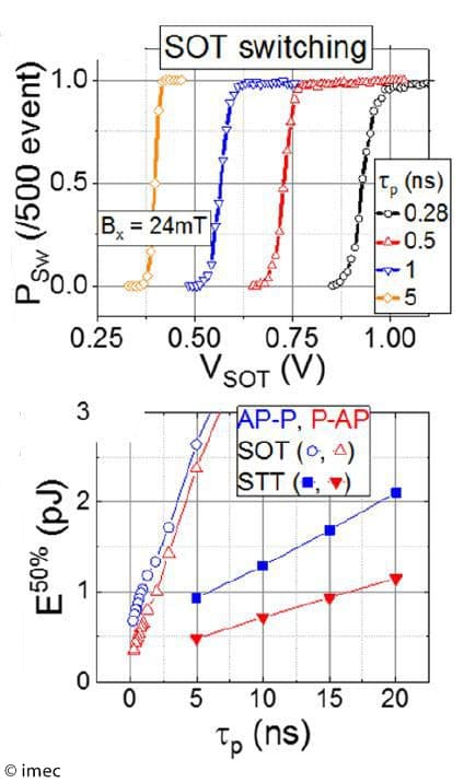
Demonstration of SOT switching: (top) switching distribution as a function of pulse voltage for various pulse lengths; (bottom) energy vs. time showing ultrafast and low-power SOT device performances.
About imec
Imec is the world-leading research and innovation hub in nanoelectronics and digital technologies. The combination of our widely acclaimed leadership in microchip technology and profound software and ICT expertise is what makes us unique. By leveraging our world-class infrastructure and local and global ecosystem of partners across a multitude of industries, we create groundbreaking innovation in application domains such as healthcare, smart cities and mobility, logistics and manufacturing, energy and education.
As a trusted partner for companies, start-ups and universities we bring together close to 4,000 brilliant minds from over 85 nationalities. Imec is headquartered in Leuven, Belgium and has distributed R&D groups at a number of Flemish universities, in the Netherlands, Taiwan, USA, China, and offices in India and Japan. In 2017, imec's revenue (P&L) totaled 546 million euro. Further information on imec can be found at www.imec-int.com.
Imec is a registered trademark for the activities of IMEC International (a legal entity set up under Belgian law as a "stichting van openbaar nut”), imec Belgium (IMEC vzw supported by the Flemish Government), imec the Netherlands (Stichting IMEC Nederland, part of Holst Centre which is supported by the Dutch Government), imec Taiwan (IMEC Taiwan Co.) and imec China (IMEC Microelectronics (Shanghai) Co. Ltd.) and imec India (Imec India Private Limited), imec Florida (IMEC USA nanoelectronics design center).
Contact
Hanne Degans, press communications manager, +32 16 28 17 69 // +32 486 06 51 75 // Hanne.Degans@imec.be
Discover more



Imec and Diraq demonstrate first coherent operation of eight silicon MOS spin qubits fabricated in a 300mm CMOS-compatible foundry process
Read more


Neural telemetry breakthrough: new chip delivers ten-fold compression while preserving signal integrity
Read more

