Imec and Unisantis Unveil Ultra-Scaled EUV-Enabled Surrounding Gate Transistor SRAM Cell
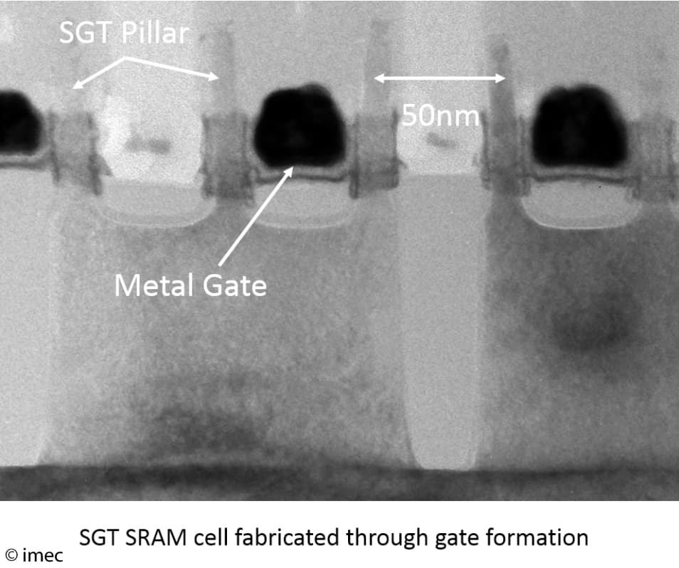
Antwerp (BELGIUM), MAY 23, 2018 – At this week’s Imec Technology Forum (ITF 2018) in Antwerp, imec, the world-leading research and innovation hub in nano-electronics and digital technology, and Unisantis Electronics Singapore Pte Ltd ( Unisantis ), a leading developer of Surrounding Gate Transistor (SGT) semiconductor technology, announce significant progress in the joint development of a process flow targeting an SGT 6T-SRAM cell with areas between 0.0184 and 0.0205 square micrometer, meeting or exceeding the dense cell area in a N5 technology node. Studies show that the vertical gate-all-around SGT-based cells have a 20-30% reduced area compared to horizontal gate-all-around FETs, while also outperforming these in terms of operating voltage, standby leakage and stability.
The Surrounding Gate Transistor is a vertical gate-all-around architecture that was developed at Unisantis as the basis for a universal silicon technology platform for DRAM, NAND, Flash, and SRAM.
“SGTs have all the advantages of horizontal gate-all-around transistors, allowing a near-perfect electrostatic control of the transistor channel,” says Professor Fujio Masuoka, Director and CTO at Unisantis and inventor of the SGT concept. “But because the channel is a vertical pillar, the concept has the potential for a significant area reduction compared to horizontal nanowire-based transistors.”
Imec and Unisantis worked out the key process flow and steps for a 6T-SRAM cell using SGT. Through a novel Design process Technology Co-Optimization (DTCO), the researchers were able to develop an SRAM bit-cell area of 0.0205 square micrometer, using a minimum pillar pitch of 50nm. This is a 24 percent improved scaling factor compared to the smallest SRAM designs published to date, and makes the design ready for an N5 technology node. A key technical challenge that was solved involved the mechanical stability of the pillars at the high aspect ratios that were required. Through the use of single-exposure EUV lithography, the number of process steps could be reduced, resulting in an estimated cost comparable to that of FinFET-based SRAM.
“We’re excited to present the results of this joint project,” says Dan Mocuta, the Logic Device and Integration department director at imec. “In a concerted effort and using the tools and expertise available in house, the imec and Unisantis engineers were able to design and are well on their way to fabricating these record-scaled SRAM cells. This again proves the value of our expertise for R&D collaborations, as well as the leading-edge abilities of our cleanroom platform.”
About imec
Imec is the world-leading research and innovation hub in nano-electronics, energy and digital technologies. The combination of our widely acclaimed leadership in microchip technology and profound software and ICT expertise is what makes us unique. By leveraging our world-class infrastructure and local and global ecosystem of partners across a multitude of industries, we create groundbreaking innovation in application domains such as healthcare, smart cities and mobility, logistics and manufacturing, and energy.
As a trusted partner for companies, start-ups and universities we bring together more than 4,000 brilliant minds from over 85 nationalities. Imec is headquartered in Leuven, Belgium and also has distributed R&D groups at a number of Flemish universities, in the Netherlands, Taiwan, USA, China, and offices in India and Japan. In 2017, imec's revenue (P&L) totaled 546 million euro. Further information on imec can be found at www.imec-int.com.
Imec is a registered trademark for the activities of IMEC International (a legal entity set up under Belgian law as a "stichting van openbaar nut”), imec Belgium (IMEC vzw supported by the Flemish Government), imec the Netherlands (Stichting IMEC Nederland, part of Holst Centre which is supported by the Dutch Government), imec Taiwan (IMEC Taiwan Co.) and imec China (IMEC Microelectronics (Shanghai) Co. Ltd.) and imec India (Imec India Private Limited), imec Florida (IMEC USA nanoelectronics design center).
Unisantis Electronics Singapore Pte Ltd is a company based in Singapore. Dr Fujio Masuoka is the Director and CTO of Unisantis.
Contact
Hanne Degans, Press communications manager, +32 16 28 17 69// +32 486 065 175// hanne.degans@imec.be
Discover more



Imec and Diraq demonstrate first coherent operation of eight silicon MOS spin qubits fabricated in a 300mm CMOS-compatible foundry process
Read more


Neural telemetry breakthrough: new chip delivers ten-fold compression while preserving signal integrity
Read more

