Imec and Soitec Demonstrate Sequential 3D Planar Device Achieving High-Reliability at Low Temperature
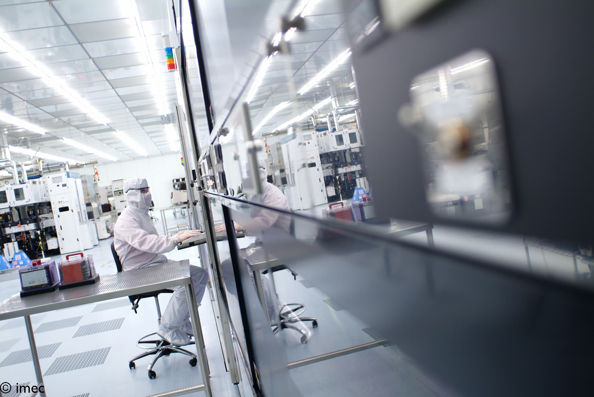
LEUVEN (Belgium), JULY 9, 2018 — Today at its annual Imec Technology Forum USA in San Francisco, imec, the world-leading research and innovation hub in nanoelectronics and digital technology, in collaboration with Soitec, leader in the design and production of innovative semiconductor materials for the electronics industry, reported that they successfully demonstrated a sequential 3D front-end integration process by stacking two device layers on one another on a 300mm wafer. This vertical integration of sequentially processed device layers, also named sequential-3D integration (S3D), is perceived as a promising alternative to continue the benefits offered by semiconductor scaling, overcoming the constraints of geometrical scaling while maintaining the benefits of functional scaling through the vertical 3D integration.
The most critical challenge of sequential-3D integration is the management of the fabrication thermal budget. To avoid or limit thermally induced device degradation issues of the bottom device layer, the top device layer must be processed at low temperatures below 525°C. The top thermal budget needs to be reduced to avoid degradation of the bottom devices, the bottom interconnects, and the bonding interface. These limitations are overcome with the implementation of junction-less transistors on the top-layer which decreases the fabrication complexity and provides sufficient device reliability.
A high device density per chip area can be realized because the alignment accuracy only depends on the lithography stepper performance and not on the accuracy of the wafer alignment, as is the case for alternative 3D-integration technologies using through-Si vias. Moreover, the sequential processing of the device layers promises a reduced length of the interconnection lines and a reduced RC delay, as compared to a 2D implementation. For efficient sequential device stacking, imec worked with Soitec's Smart CutTM technology to transfer a thin layer of crystalline material from one substrate to the substrate processed with the first layer of devices, overcoming physical limitations and opening innovative opportunities in 3D IC product design.
“Demonstrating a good performance of the top-tier device using a low temperature process is an important breakthrough in our aim to develop sequential 3D as a valid option to further increase power-performance-area-cost in advanced technology nodes beyond 5nm,” stated Anne Vandooren, senior researcher at imec. “To realize this, we had to use very advanced technologies in some of the most critical process steps including back-end-of-line, contacts, and gate stacks.”
Imec demonstrated a junction-less top device layer featuring a low fabrication complexity, which does not require junction formation, channel doping and activation performed prior to layer transfer. The top-tier device was processed at a temperature below 525°C achieving good device performance (SS =72mV/dec, DIBL=80mV/V Ioff=1pA/um Ion=220uA/um at VDD=1V), without impact from layer transfer. Moreover, a junction-less device presents the additional advantage of a reduced oxide electric field at on-state condition, which enables sufficient NBTI/PBTI reliability (10-year reliable operation at VG=Vth+0.6V, 125C), even without performing the customary high temperature “reliability anneal”.
“This exciting R&D collaboration between imec and Soitec is paving the way for global innovation,” explained Bich-yen Nguyen, Senior Fellow at Soitec. “Together we are leveraging the maturity of Soitec’s Smart Cut™ process, excellent quality and thickness control, and imec’s advanced device and integration know-how, to develop another method to meet the PPAC (Power, Performance, Area and Cost) in scaling.”
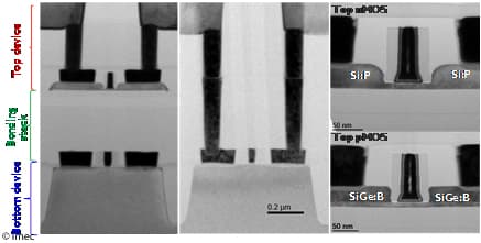
Figure 2: This chart displays data showing the reliability improvement of junction-less devices (JL) over inversion mode (IM) devices processed at low temperature. Data of optimized FinFETs with high temperature reliability anneal are reported as a reference. Depicted here are NBTI and PBTI VT shifts (DVth) measured at VG=Vth0+0.6V, T=125˚C, at a stress time of 1000s, and a sense time of 1ms.
About imec
Imec is the world-leading research and innovation hub in nanoelectronics and digital technologies. The combination of our widely acclaimed leadership in microchip technology and profound software and ICT expertise is what makes us unique. By leveraging our world-class infrastructure and local and global ecosystem of partners across a multitude of industries, we create groundbreaking innovation in application domains such as healthcare, smart cities and mobility, logistics and manufacturing, energy and education.
As a trusted partner for companies, start-ups and universities we bring together close to 4,000 brilliant minds from over 85 nationalities. Imec is headquartered in Leuven, Belgium and has distributed R&D groups at a number of Flemish universities, in the Netherlands, Taiwan, USA, China, and offices in India and Japan. In 2017, imec's revenue (P&L) totaled 546 million euro. Further information on imec can be found at www.imec-int.com.
Imec is a registered trademark for the activities of IMEC International (a legal entity set up under Belgian law as a "stichting van openbaar nut”), imec Belgium (IMEC vzw supported by the Flemish Government), imec the Netherlands (Stichting IMEC Nederland, part of Holst Centre which is supported by the Dutch Government), imec Taiwan (IMEC Taiwan Co.) and imec China (IMEC Microelectronics (Shanghai) Co. Ltd.) and imec India (Imec India Private Limited), imec Florida (IMEC USA nanoelectronics design center).
Contact
Hanne Degans, press communications manager, +32 16 28 17 69 // +32 486 06 51 75 // Hanne.Degans@imec.be
About Soitec
Soitec (Euronext, Tech 40 Paris) is a world leader in designing and manufacturing innovative semiconductor materials. The company uses its unique technologies and semiconductor expertise to serve the electronics market. With more than 3,000 patents worldwide, Soitec’s strategy is based on disruptive innovation to answer its customers’ needs for high performance, energy efficiency and cost competitiveness. Soitec has manufacturing facilities, R&D centers and offices in Europe, the U.S. and Asia. For more information, please visit www.soitec.com and follow us on Twitter: @Soitec_EN
Soitec and Smart Cut are registered trademarks of Soitec.
Contact
Erin Berard, +33 6 80 36 53 40 // erin.berard@soitec.com
Discover more



Imec and Diraq demonstrate first coherent operation of eight silicon MOS spin qubits fabricated in a 300mm CMOS-compatible foundry process
Read more


Neural telemetry breakthrough: new chip delivers ten-fold compression while preserving signal integrity
Read more

