Imec and partners report major breakthroughs for spintronic logic devices in two different implementations

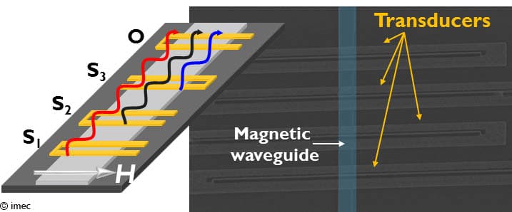
SAN FRANCISCO (USA), DECEMBER 3, 2018 — This week, at the 2018 IEEE International Electron Devices Meeting (IEDM), imec, the world-leading research and innovation hub in nano-electronics and digital technology, and its partners present the first experimental demonstration of full majority gate operation based on spin-wave interference in scaled devices. Circuit-level benchmarking recommends majority gates based on spin-waves for ultralow power applications. Imec also demonstrated the first logic gate implementation based on magnetic domain wall propagation. Fully integrated logic devices were fabricated on 300mm wafers using CMOS compatible processes. These breakthroughs constitute the foundation of a robust spintronics platform that will be used for functional spintronic logic components for low-power applications.
In the quest for low-power electronics, imec is investigating majority gates based on spintronics phenomena as a possible path towards more efficient circuits. Majority gates are ‘democratic’ devices that return true if more than 50% of their inputs are true. Complex logic operation such as addition and multiplication can be emulated in a much more compact and energy efficient way than with the conventional NAND-based circuits. Imec now reports breakthroughs for two different implementations of majority gates. Both implementations are based on spintronics, which exploits the magnetization state in a ferromagnet rather than the charge of electrons to perform logic operations.
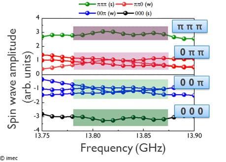
A first breakthrough is reported for devices that use the interference of spin waves to enable logic operation. While basic functionality was shown earlier for large-scale devices, imec, in collaboration with University Paris-Sud, has for the first time experimentally demonstrated full majority gate operation in sub-µm devices. The research team has verified the full truth table of a majority logic function, which lists all possible configurations of the input variables together with the result of the operation of those values. They also demonstrated the ability to distinguish between strong and weak majority, making these devices attractive for neuromorphic applications.
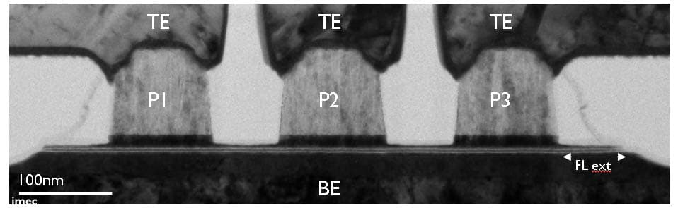
The second breakthrough is reported for devices based on magnetic domain wall generation and propagation, another spintronics phenomenon. Imec, in collaboration with Intel and University Paris-Sud reports first logic function demonstration based on domain wall propagation. For the first time, it was demonstrated the nucleation, propagation, and detection of magnetic domain walls with magnetic tunnel junctions connected by a free layer ferromagnet. The domain walls are generated via spin transfer torque. The motion of the domain walls was monitored and verified via tunnel magnetoresistance measurements through a series of adjacent magnetic tunnel junctions which share the free layer. The devices were fabricated on 300mm wafers using CMOS compatible production processes. Imec’s capability to pattern these delicate structures is a key enabler for the fabrication process.
Imec’s research into advanced logic scaling is performed in cooperation with imec’s key CMOS program partners including GlobalFoundries, Huawei, Intel, Micron, Qualcomm, Samsung, SK Hynix, Sony Semiconductor Solutions, TOSHIBA Memory, TSMC and Western Digital.
About imec
Imec is the world-leading research and innovation hub in nanoelectronics and digital technologies. The combination of our widely acclaimed leadership in microchip technology and profound software and ICT expertise is what makes us unique. By leveraging our world-class infrastructure and local and global ecosystem of partners across a multitude of industries, we create groundbreaking innovation in application domains such as healthcare, smart cities and mobility, logistics and manufacturing, energy and education.
As a trusted partner for companies, start-ups and universities we bring together more than 4,000 brilliant minds from over 85 nationalities. Imec is headquartered in Leuven, Belgium and has distributed R&D groups at a number of Flemish universities, in the Netherlands, Taiwan, USA, China, and offices in India and Japan. In 2017, imec's revenue (P&L) totaled 546 million euro. Further information on imec can be found at www.imec-int.com.
Imec is a registered trademark for the activities of IMEC International (a legal entity set up under Belgian law as a "stichting van openbaar nut”), imec Belgium (IMEC vzw supported by the Flemish Government), imec the Netherlands (Stichting IMEC Nederland, part of Holst Centre which is supported by the Dutch Government), imec Taiwan (IMEC Taiwan Co.) and imec China (IMEC Microelectronics (Shanghai) Co. Ltd.) and imec India (Imec India Private Limited), imec Florida (IMEC USA nanoelectronics design center).
Discover more



Imec and Diraq demonstrate first coherent operation of eight silicon MOS spin qubits fabricated in a 300mm CMOS-compatible foundry process
Read more


Neural telemetry breakthrough: new chip delivers ten-fold compression while preserving signal integrity
Read more

