Imec and ASML Enter Next Stage of EUVL Collaboration
Intensified collaboration will advance high-volume production with current EUV lithography (EUVL) and develop future EUV systems
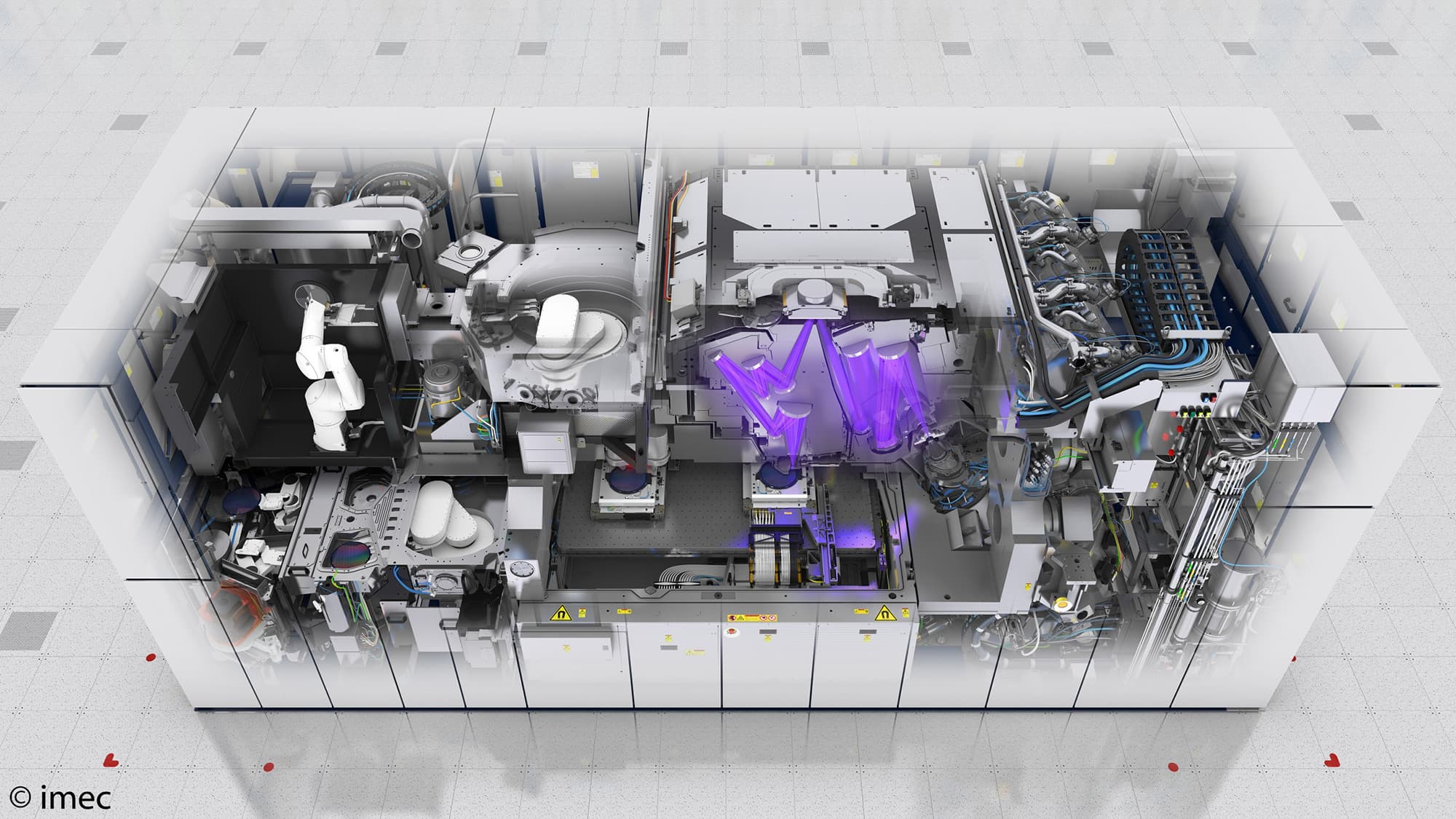
LEUVEN (Belgium) & VELDHOVEN (The Netherlands), OCTOBER 22, 2018 —Today, world-leading research and innovation hub in nanoelectronics and digital technologies imec, and ASML Holding N.V. (ASML), the technology and market leader in lithographic equipment, announce the next step in their extensive collaboration. Together, they will accelerate the adoption of EUV lithography for high-volume production, including the current latest available equipment for EUV (0.33 Numerical Aperture, NA). Moreover, they will explore the potential of the next-generation high-NA EUV lithography to enable printing of even smaller nanoscale devices advancing semiconductor scaling towards the post 3 nanometer Logic node. To this end, they will establish a joint high-NA EUV research lab.
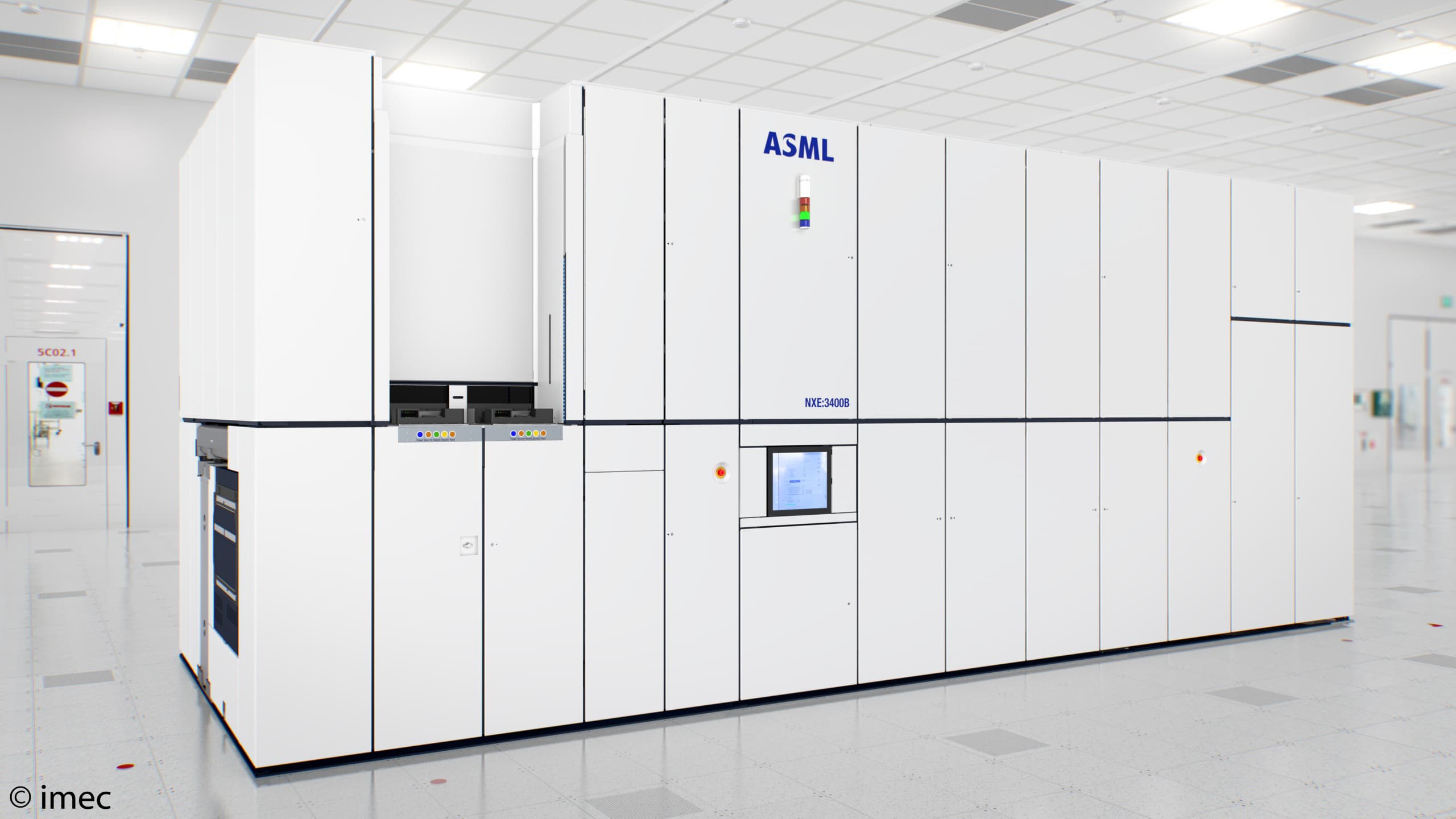
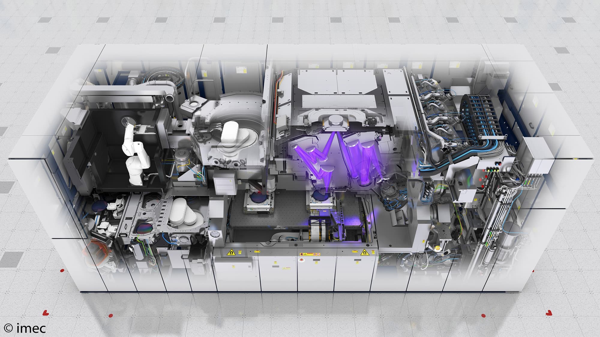
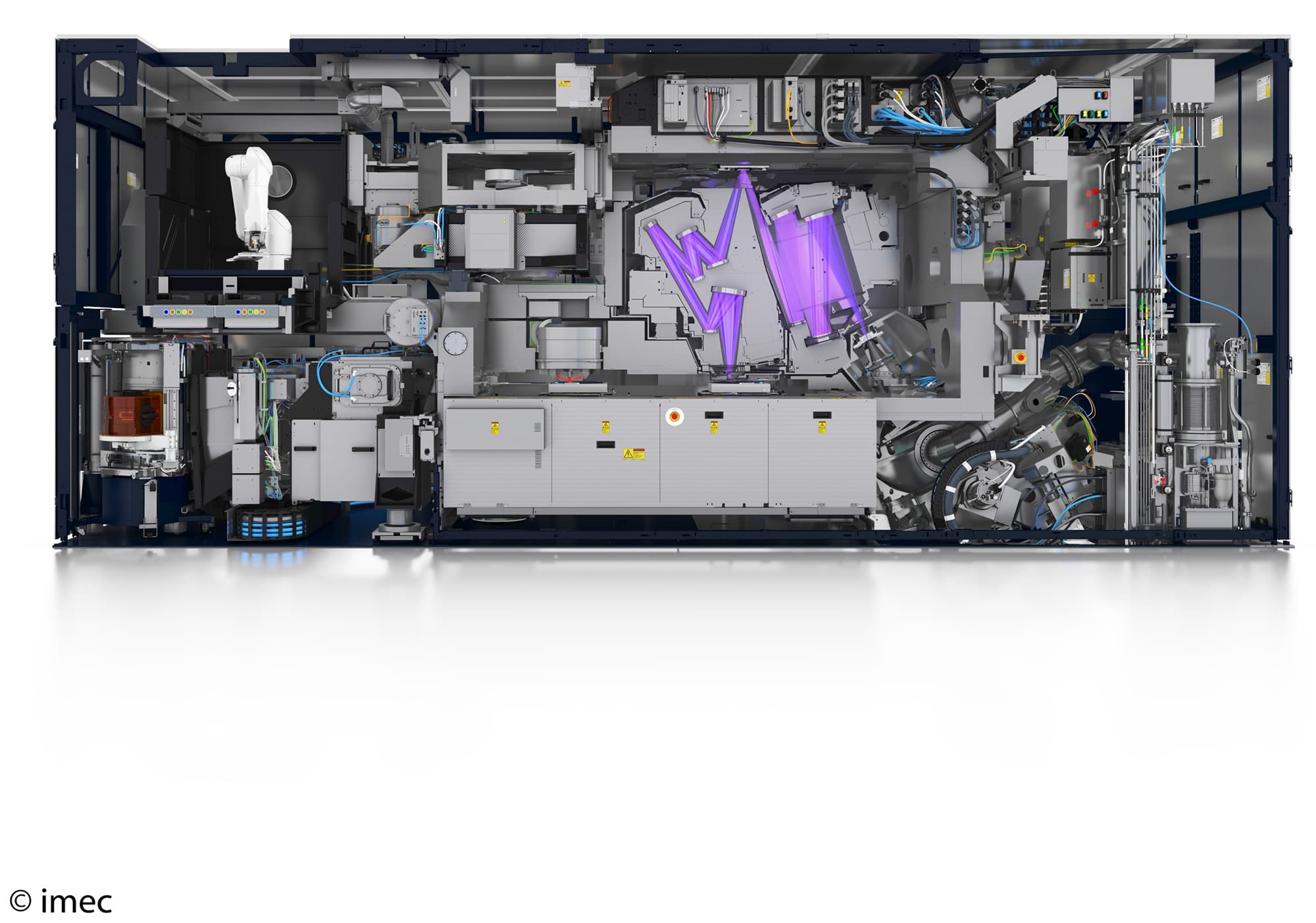
Imec and ASML have been conducting joint research for almost thirty years. In 2014, they created a joint research center, the Advanced Patterning Center, to optimize lithography technology for advanced CMOS integration and to prepare the ecosystem to support advance patterning requirements. Now, they bring this cooperation to the next stage with the installation of ASML’s most advanced and high-volume production dedicated EUV scanner (NXE:3400B) in imec’s cleanroom. Utilizing imec’s infrastructure and advanced technology platforms, imec and ASML researchers and partner companies can pro-actively analyze and solve technical challenges such as defects, reliability and yield, and as such accelerate the EUV technology’s industrialization.
With a 250W light source, ASML’s newest EUV system throughput will be more than 125 wafers per hour, one of the industry’s most important requirements for high-volume production. The NXE:3400B will also be equipped with the latest alignment and leveling sensors, to enable optimal process control at this high throughput. This will facilitate the overlay matching of the NXE:3400B to that of the latest immersion scanner, NXT:2000i, that will also be installed in imec’s cleanroom in 2019. In addition, ASML and imec will expand the metrology capability with new ASML YieldStar optical metrology and ASML-HMI Multi-electron beam metrology equipment, allowing more accurate and faster evaluation of nanoscale structures.
To continue on the leading edge of lithography development, a second component of the increasing collaboration is the foundation of a joint high-NA EUV research lab. In this lab, researchers from both organizations will experiment with the next generation of EUV lithography at higher NA. Systems with a higher NA project the EUV light onto the wafer under larger angles, improving resolution, and enabling printing of smaller features. More specifically, the new high-NA EUV system, EXE:5000, that will be installed in the joint research lab, will have an NA of 0.55 instead of 0.33 in current NXE:3400 EUV systems. Already now, the first joint scientific projects to facilitate the introduction of high-NA EUV, are ongoing. In the joint research lab, ASML and imec will perform research on the manufacturing of the most advanced nanoscale devices by high-NA EUV and assist the ecosystem of equipment and material suppliers to prepare for the introduction of high-NA EUV technology to the industry.
Luc Van den hove, President and CEO of imec: “The new EUV scanners and ASML metrology equipment will allow our industry partners to perform collaborative research on the most advanced and industry relevant lithography and metrology equipment. When it comes to lithography, ASML is undoubtedly the world leader. ASML and imec have a nearly 30 year long tradition of joint research, leading to breakthrough patterning research to advance the semiconductor industry roadmap.”
Martin van den Brink, President & Chief Technology Officer at ASML: “We are very pleased to take this next step in our long and deep collaboration with imec. Access to the most advanced semiconductor lithography tools is vital for exploration and determining the paths to future generations of semiconductor devices and applications. Imec’s researchers and customers can be sure of the most up to date holistic lithography technology for many years to come. The semiconductor industry and consumers and businesses around the world will benefit from the fruits of imec’s work over the next decade, resulting in continuing improvements in microchip cost and performance.”
About imec
Imec is the world-leading research and innovation hub in nanoelectronics and digital technologies. The combination of our widely acclaimed leadership in microchip technology and profound software and ICT expertise is what makes us unique. By leveraging our world-class infrastructure and local and global ecosystem of partners across a multitude of industries, we create groundbreaking innovation in application domains such as healthcare, smart cities and mobility, logistics and manufacturing, energy and education.
As a trusted partner for companies, start-ups and universities we bring together more than 4,000 brilliant minds from over 85 nationalities. Imec is headquartered in Leuven, Belgium and has distributed R&D groups at a number of Flemish universities, in the Netherlands, Taiwan, USA, China, and offices in India and Japan. In 2017, imec's revenue (P&L) totaled 546 million euro. Further information on imec can be found at www.imec-int.com.
Imec is a registered trademark for the activities of IMEC International (a legal entity set up under Belgian law as a "stichting van openbaar nut”), imec Belgium (IMEC vzw supported by the Flemish Government), imec the Netherlands (Stichting IMEC Nederland, part of Holst Centre which is supported by the Dutch Government), imec Taiwan (IMEC Taiwan Co.) and imec China (IMEC Microelectronics (Shanghai) Co. Ltd.) and imec India (Imec India Private Limited), imec Florida (IMEC USA nanoelectronics design center).
About ASML
ASML is one of the world’s leading manufacturers of chip-making equipment. Our vision is a world in which semiconductor technology is everywhere and helps to tackle society’s toughest challenges. We contribute to this goal by creating products and services that let chipmakers define the patterns that integrated circuits are made of. We continuously raise the capabilities of our products, enabling our customers to increase the value and reduce the cost of chips. By helping to make chips cheaper and more powerful, we help to make semiconductor technology more attractive for a larger range of products and services, which in turn enables progress in fields such as healthcare, energy, mobility and entertainment. ASML is a multinational company with offices in 60 cities in 16 countries, headquartered in Veldhoven, the Netherlands. We employ more than 21,000 people on payroll and flexible contracts (expressed in full time equivalents). ASML is traded on Euronext Amsterdam and NASDAQ under the symbol ASML. More information about ASML, our products and technology, and career opportunities is available on www.asml.com.
Discover more



Imec and Diraq demonstrate first coherent operation of eight silicon MOS spin qubits fabricated in a 300mm CMOS-compatible foundry process
Read more


Neural telemetry breakthrough: new chip delivers ten-fold compression while preserving signal integrity
Read more

