Gian Lorusso
Gian F. Lorusso received his PhD in solid state physics from the University of Bari, Italy, in 1992. He has been working on topics related to the semiconductor industry such as metrology tool development, lithography, material analysis and more. His domains of expertise include lithography, metrology, microscopy, and spectrometry. He worked at the École Polytechnique Fédérale de Lausanne (Switzerland), the Center for X-ray Lithography (Wisconsin), the Center for X-ray Optics at Lawrence Berkeley National Laboratories (California), and KLA-Tencor (California). He joined imec (Belgium) in 2006. His work has produced more than 200 papers and 15 patents. He is working on Extreme Ultraviolet Lithography and Metrology, fields in which he started in the early nineties.

Authored articles
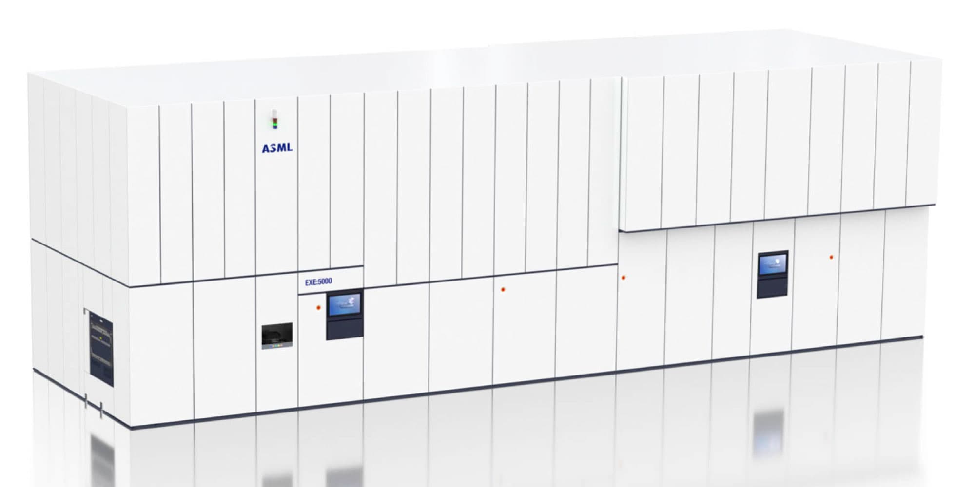
High-NA EUV lithography: the next major step forward
In the course of 2025, we expect to see the introduction of the first high-NA extreme ultraviolet lithography (EUVL) equipment in high-volume manufacturing environments. These next-generation lithography systems will be key to advance Moore’s Law towards the logic 2nm technology generation and beyond. In this article, imec scientists and engineers involved in preparing this major engineering project (in partnership with ASML) talk about challenges and opportunities. They highlight recent insights. And they discuss the progress made in developing the patterning processes, metrology and photomasks needed for enabling the high-NA EUV lithography infrastructure.
Read more