Here is that good old roll of film again
No, we’re not talking about the roll of film in your old analogue camera. What we mean here is a digital ‘roll of film’ that one can use to make X-ray images, fingerprint and palm scans, or inspection cameras that fit round a pipe. Pawel Malinowski, program manager at imec’s thin-film electronics group and Florian De Roose, researcher at imec, tell us more about the technology they are developing with fellow researchers from Holst Centre.

What you can do with a thin layer of electronics and photodiodes
If you cover a plastic film or glass plate with thin layers of specific materials, it is possible to create electrical circuits and photodiodes. For the electronics (thin-film transistors) you can use metal oxide and for the photodiodes there are perovskites, organic molecules or quantum dots. Image sensors produced in this way are both semi-transparent and flexible (if they’re on a plastic film) and also relative cheap. Plus you can produce them in very large sizes. But what can these large, semi-transparent, cheap and flexible photo surfaces be used for?
An obvious first application is in the medical sector. To obtain X-ray images, you still have to go to the radiology department at a hospital. But thin-film image sensors make it possible to create portable X-ray devices that are a lot lighter – and cheaper – than existing versions (they’re unbreakable, too, if they’re made on a plastic film).
Fingerprints and palm prints can be used to identify a person. Such scans can also be made with thin-film image sensors. For example, if you lay a thin layer of these image sensors on your full smartphone screen, you can secure every app on your homescreen using your fingerprint. Or if you wrap this image sensor film round a door handle or the grip of a drill, then only you can open the door or use the drill, based on your palm print.
And if you cover a glazed surface (a wall or floor) with thin-film image sensors, you can detect gestures or shadows. Which can be very interesting for smart buildings.
Finally, you can also wrap image sensor surfaces around anything, such as round a pipeline or an aircraft wing, so that it can be inspected easily for aging, leaks, cracks and so on.
Possible applications of large, semi-transparent, cheap and flexible photo surfaces based on thin-film transistors and photodiodes
Ready for the FBI
During an important Display conference (SID) in Los Angeles at the end of May, imec and Holst Centre exhibited their fingerprint and palm sensor based on thin-film image sensors. The film is only 0.2 mm thick and can be used to conduct an identity check on objects of any kind. That might be a door handle, a mobile phone screen, the steering wheel of a car, etc.
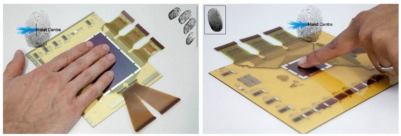
We demonstrated a first film measuring 6 by 8 cm – which can check 4 fingers simultaneously – and which has a resolution of 200ppi. The second film – designed for a single fingerprint – has a resolution of 500ppi. This level of accuracy is what would be typical for the FBI to identify someone correctly.
The image sensors detect visible light between 400 and 700 nm that is reflected by the skin. They can also detect light that penetrates the skin before being reflected. This latter feature is of value for detecting a heartbeat, which provides an extra security check.
The fingerprint and palm print sensor is made up of a layer of oxide thin-film transistors with organic photodiodes on top. These photodiodes can then be ‘tuned’ by using a different organic material so that they detect a different wavelength, such as near infrared. This enables the vein pattern in a hand to be visualized, which is even more precise for accurate identification than a palm print.
In addition to this fingerprint scanner based on photodiodes and light, imec and Holst Centre are also working on a scanner that uses thermal sensors (PYCSEL project). Once again a lower layer of oxide thin-film transistors is used. The upper layer is a material that measures electric temperature changes. The fingerprint is then detected indirectly by local variations in temperature changes that correspond with the pattern of the fingerprint. Here again a resolution of 500ppi is achievable.
Portable X-ray machine
The digital X-ray machines available today are definitely a huge step forward compared with their analog counterparts. Yet they’re still not ideal. For a start, they are relatively expensive – and frequently too expensive for developing countries – and the resolution could also be better. Typically, a “thick-layer scintillator” is used to convert the X-rays into light, which then hits the image sensors and is processed further. The light that passes through the scintillator is diffused in multiple directions, which results in part of the information from the X-rays being lost.
Together with partners from the DiCoMo project, imec has developed a new type of digital X-ray machine that is lighter, safer (because of the lower level of X-rays), more robust and more sensitive. This makes a great contribution in the evolution towards safe, portable X-ray machines that can simply be used in the patient’s room.
A demonstrator has been produced with 640 x 480 pixels and a resolution of 254ppi. It features a lower layer of metal oxide thin-film transistors with a photoactive layer on top. This produces less light diffusion than in existing digital X-ray scanners.
In another project – NEXIS – multiple layers of thin-film photodiodes are stacked on top of each other, with each layer sensitive to a different wavelength. This generates an X-ray scan that provides a great deal more information than traditional systems. It also means that an X-ray scanner can be used to diagnose and monitor a stroke or heart attack. A truly portable X-ray scanner has many advantages, of course, because it can be used in the treatment room itself. This saves time and means that the patient can be treated more quickly.
In the next stage of the research, the X-ray film will be made bigger using a stable production process that can be transferred later to industry

Imec is investigating – along with material manufacturers – possible materials for thin-film image sensors: oxides, perovskites, quantum dots, small organic molecules, etc. The many years of experience gained in imec’s solar cell group – which produces thin-film solar cells – also come in handy here. Imec is looking at various integration possibilities, with thin-film photodiodes in particular being integrated onto thin-film electronics or silicon electronics. The choice in this instance is made taking into account the requirements of the specific application.
The research into thin-film electronics, displays and image sensors is being conducted in conjunction with Holst Centre, which was established in 2005 by imec and TNO. Holst Centre has its own GEN1 pilot line in which technologies can be tested on an industrial scale and on professional devices. In fact, the aim is to produce thin-film technology on roll-to-roll printers, using large pieces of film.
A special thank you
Special thanks to Hylke B. Akkerman (Holst Centre) and the OPD and GEN1 teams at Holst Centre, as well as to David Cheyns (imec) and the thin-film team at imec for their work in thin-film imaging, as detailed in this article.
Want to know more?
- Like to read the paper ‘Thin-Film Quantum Dot Photodiode for Monolithic Infrared Image Sensors’ en ‘A Flexible Thin-Film Pixel Array with a Charge-to-Current Gain of 59μA/pC and 0.33% Nonlinearity and a Cost Effective Readout Circuit for Large-Area X-ray Imaging’? Let us know via this contact form.
- DiCoMo is a European Horizon 2020 project. To learn more about the project and the consortium partners, visit this website. This project has received funding from the European Union’s Horizon 2020 research and innovation program as part of the H2020-ICT-2014-1 call under grant agreement nr. 643920.
- Nexis is a European Horizon 2020 project. To learn more about the project and the consortium partners, visit this website. This project has received funding from the European Union's Horizon 2020 Research and Innovation Program under Grant Agreement nr. 780026.
- Pycsel is a European Horizon 2020 project. This project has received funding from the European Union’s H2020 Program under grant agreement nr. 732423
Authors

Pawel Malinowski
Pawel E. Malinowski obtained his MSc in electronics and telecommunications, specializing in radiation-tolerant integrated circuits, from Lodz University of Technology, Poland, in 2006. He completed his Ph.D. in electrical engineering at KU Leuven, Belgium, in 2011, focusing on III-nitride-based imagers for space applications. Since 2011, he has been a senior researcher and program manager in the Sensor and Actuator Technologies Department at imec.
His research spans emerging photodetectors, image sensors, and high-resolution OLED displays. Pawel has authored/co-authored over 80 publications and received awards including the International Display Workshops Best Paper Award in 2014 and the SID Display Week 2018 Distinguished Paper Award.

Florian De Roose
Florian De Roose received his M.S. degrees in electrical engineering from KULeuven, Leuven., Belgium in 2013. Afterwards, he joined the research team towards advanced thin-film applications at the Thin-Film Electronics group of imec. Concurrently he is also part of the MICAS group of the KULeuven as a PhD researcher on advanced mixed-signal design in a-IGZO thin-film technology on flex. His research interests include display design, NFC and sensor readout on flex and large area imaging, with special interest in system design of large area applications and the corresponding technology constraints.
Discover more



Imec and Diraq demonstrate first coherent operation of eight silicon MOS spin qubits fabricated in a 300mm CMOS-compatible foundry process
Read more


Neural telemetry breakthrough: new chip delivers ten-fold compression while preserving signal integrity
Read more

