Imec reports monolithic thin-film image sensor for the SWIR range with record pixel density

21/10/2019
Automotive

Achievement enables high resolution applications in surveillance, biometric identification, virtual reality, research, and industrial automation

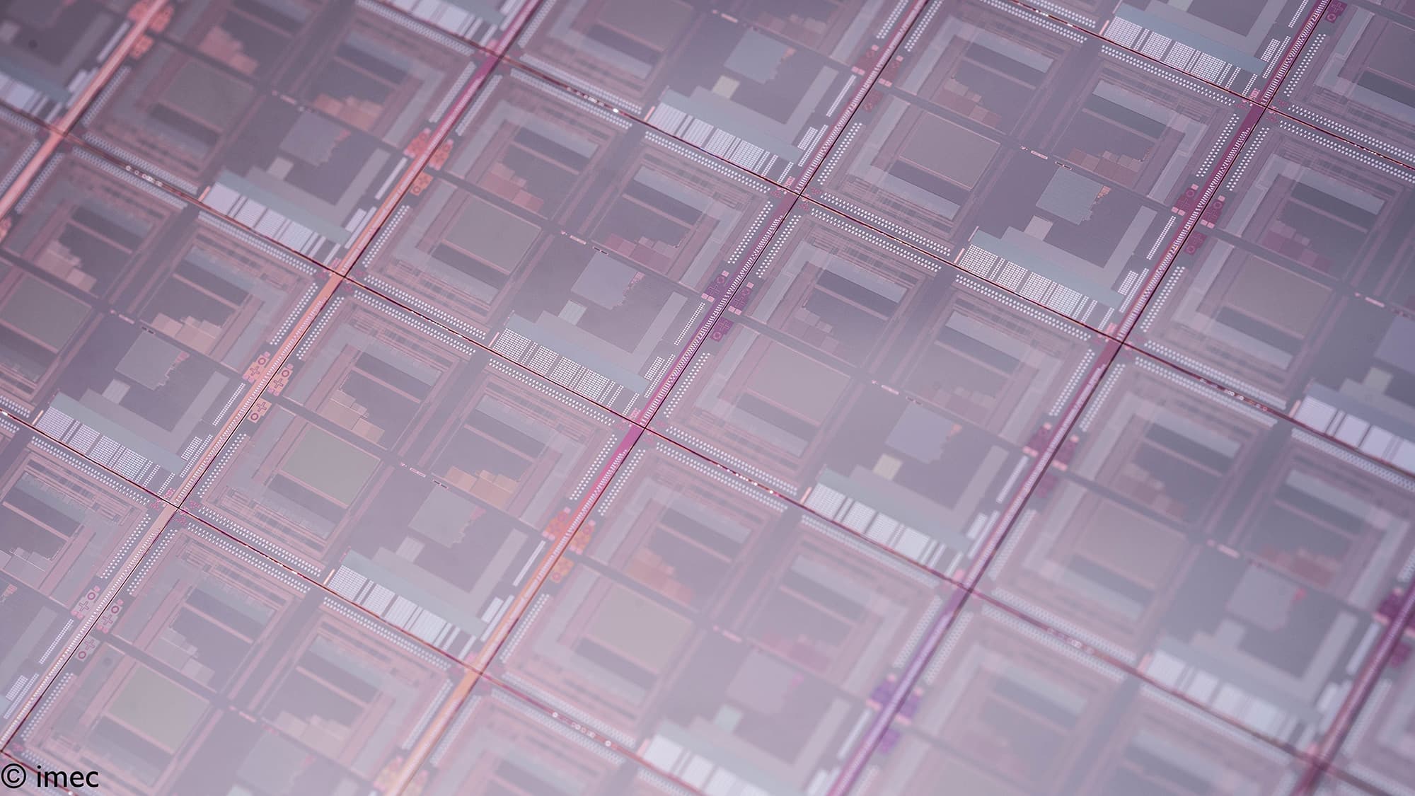
Close-up of a patterned semiconductor wafer with repeated square chip structures
Wafer with patterned SWIR image sensors
Wafer with image sensors for the SWIR range. Processed at wafer-scale, these thin-film imagers can be produced with increased throughput and cost compared to today’s conventional IR imagers, while at the same time enabling multi-megapixel resolution
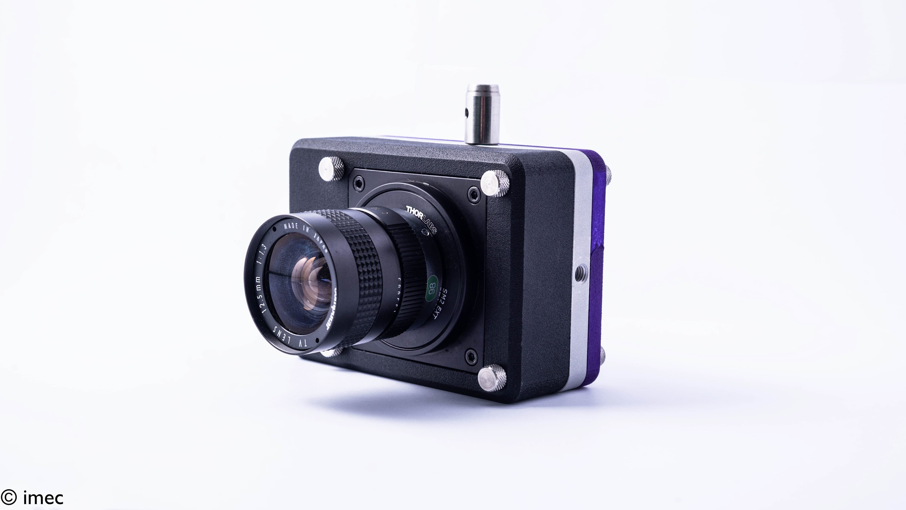
Compact camera module with a large lens attached to a black sensor housing on a white background
Imec’s thin-film SWIR image sensors can be integrated in camera modules with standard or SWIR lenses.
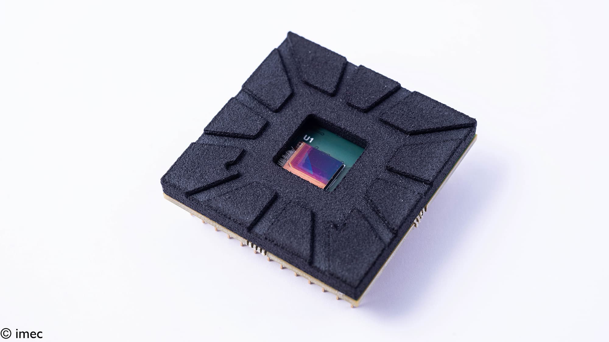
Thin-film SWIR image sensor chip with a central exposed die on a white background
Monolithic thin-film image sensor for the SWIR range, processed at die level. Imec works towards scaling the process to wafer level which increases throughput and cost compared to today’s conventional IR imagers, while at the same time enabling multi-megapixel resolution.
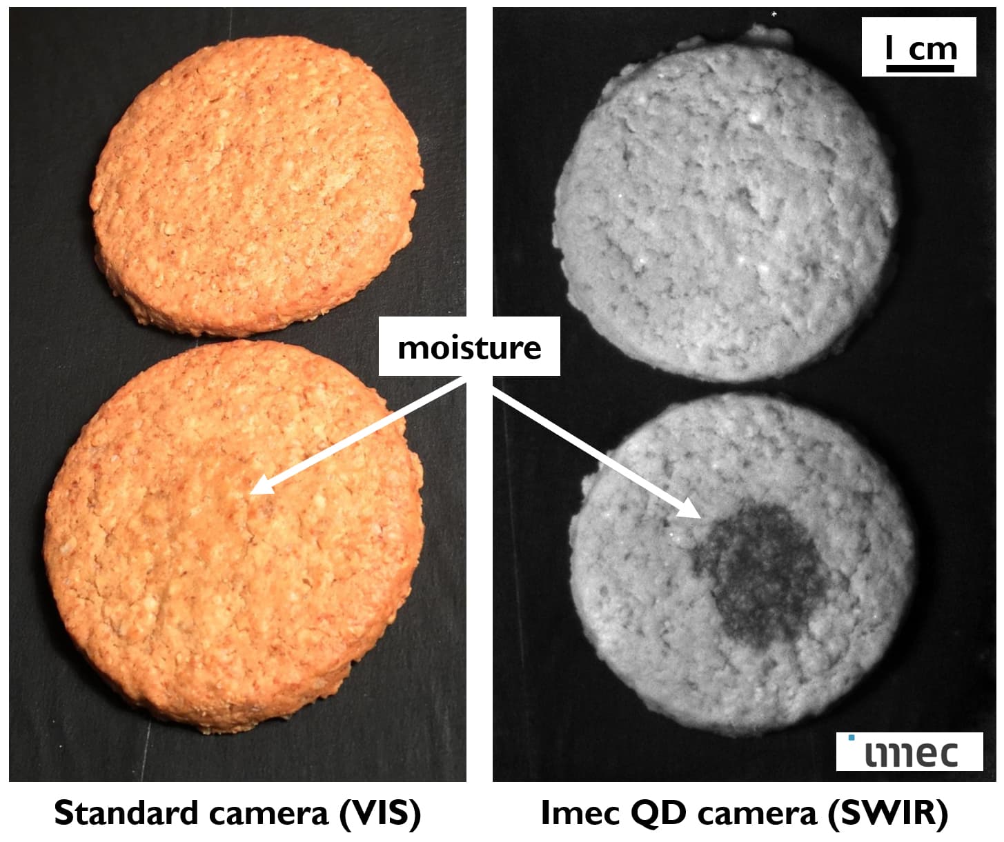
Side-by-side visible and SWIR cookie images showing moisture as a dark spot in the lower cookie
Test images of cookies acquired with a standard Si-based camera in visible range (left) and imec QD-based camera at the wavelength of 1450 nm (right). Bottom cookie had a drop of water applied to its surface, which can be only distinguished in the SWIR thanks to high water absorption contrast.

About imec


Imec is a world-leading research and innovation hub in nanoelectronics and digital technologies. The combination of our widely acclaimed leadership in microchip technology and profound software and ICT expertise is what makes us unique. By leveraging our world-class infrastructure and local and global ecosystem of partners across a multitude of industries, we create groundbreaking innovation in application domains such as healthcare, smart cities and mobility, logistics and manufacturing, energy and education.

As a trusted partner for companies, start-ups and universities we bring together more than 4,000 brilliant minds from over 97 nationalities. Imec is headquartered in Leuven, Belgium and has distributed R&D groups at a number of Flemish universities, in the Netherlands, Taiwan, USA, and offices in China, India and Japan. In 2018, imec's revenue (P&L) totaled 583 million euro. Further information on imec can be found at www.imec-int.com.

Imec is a registered trademark for the activities of IMEC International (a legal entity set up under Belgian law as a "stichting van openbaar nut”), imec Belgium (IMEC vzw supported by the Flemish Government), imec the Netherlands (Stichting IMEC Nederland, part of Holst Centre which is supported by the Dutch Government), imec Taiwan (IMEC Taiwan Co.) and imec China (IMEC Microelectronics (Shanghai) Co. Ltd.) and imec India (Imec India Private Limited), imec Florida (IMEC USA nanoelectronics design center).

Discover more

3D illustration of a modular chiplet package with several stacked semiconductor blocks on a blue background

From horsepower to high-performance compute: automotive chiplets take the leap towards autonomous edge computing

28/05/2026
Vision
Automotive
Read more
Cars driving through a city street at sunset with an overlaid sensor-network graphic

SENSAI: digital twin for next-gen automotive sensors

Page
Automotive
Artificial intelligence
Read more
Stylized automotive chiplet with glowing orange circuit traces on a dark background

Arm: a partner spotlight on imec’s Automotive Chiplet Program (ACP)

15/04/2026
Automotive
Read more
3D illustration of a modular chiplet package on a blue background

Autonomous edge chiplet program

Page
Automotive
Logic devices
Read more
Groene lichtpuntjes verspreid over horizontale lagen, als een abstract beeld van vloeistofgeheugen

Next-gen UWB radio technology to enable radar sensing, data streaming, and advanced ranging applications

07/01/2026
Research update
Ultra-wide band
Automotive
Read more
Four executives pose for a group photo in front of a presentation screen

Strategic alignment between imec and Japan’s ASRA aims to harmonize standardization of automotive chiplet architectures

16/12/2025
press release
Automotive
Read more
Colorful 300mm semiconductor wafer with patterned chip dies

Imec successfully integrates colloidal quantum dot photodiodes (QDPDs) on metasurfaces developed on 300mm CMOS wafers

11/12/2025
press release
Sensing and actuation
Automotive
Read more
Large group of conference attendees posing with raised hands outside IPAI Spaces beside an Automotive Chiplet Forum banner

A look back at the Automotive Chiplet Forum 2025

21/10/2025
Automotive
Read more
Glowing car model on a microchip with circuit traces, symbolizing automotive chiplet technology.

GlobalFoundries, Infineon, Silicon Box, STATS ChipPAC, TIER IV Join imec Automotive Chiplet Program

15/10/2025
press release
Automotive
Read more

imec in your region

Looking for information about imec's activities in different parts of the world?

United Kingdom
United States
Qatar